- 您現(xiàn)在的位置:買賣IC網(wǎng) > PDF目錄376597 > DDC112UK Dual Current Input 20-Bit ANALOG-TO-DIGITAL CONVERTER PDF資料下載
參數(shù)資料
| 型號: | DDC112UK |
| 英文描述: | Dual Current Input 20-Bit ANALOG-TO-DIGITAL CONVERTER |
| 中文描述: | 雙路電流輸入20位模擬數(shù)字轉(zhuǎn)換器 |
| 文件頁數(shù): | 23/24頁 |
| 文件大小: | 210K |
| 代理商: | DDC112UK |

DDC112
23
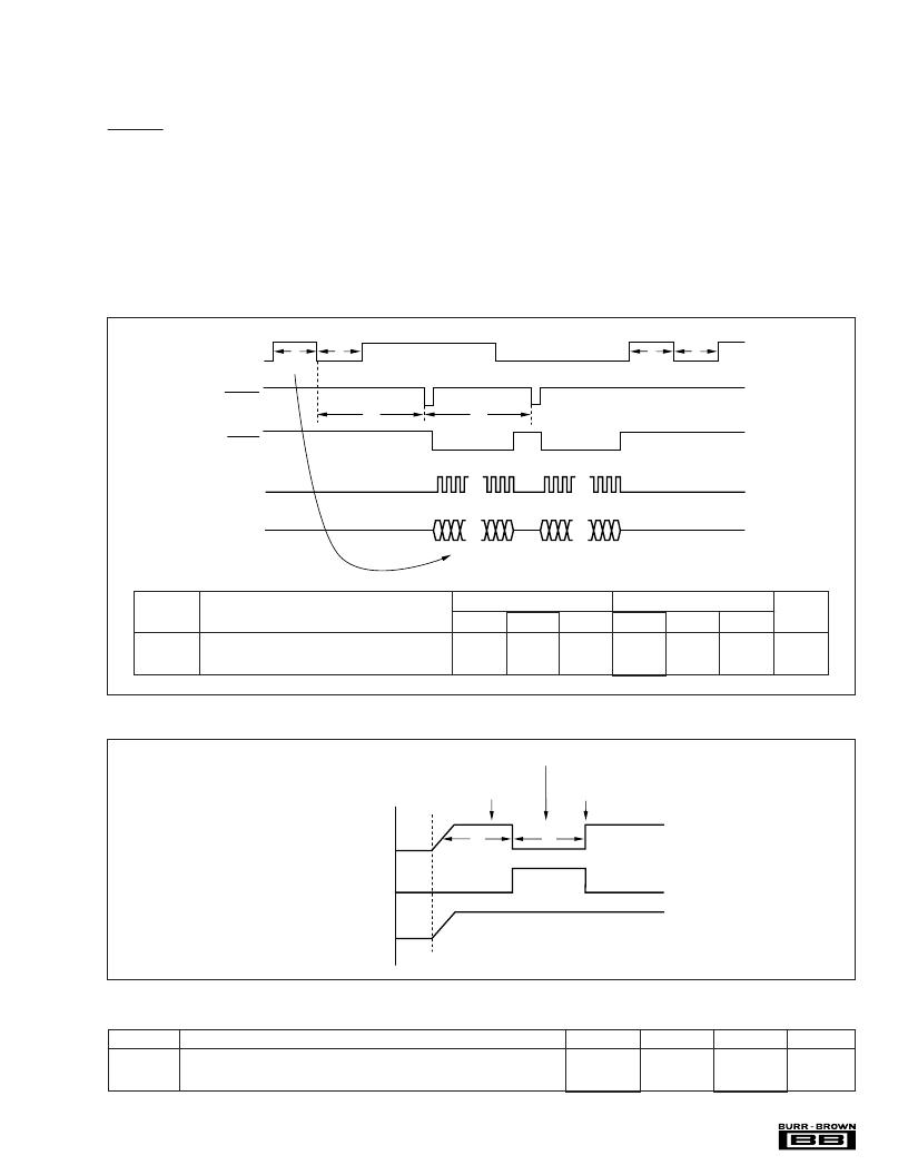
RETRIEVAL: NONCONTINUOUS MODE
Retrieving in noncontinuous mode is slightly different as
compared with the continuous mode. As shown in Figure 27
and described in detail in Application Bulletin AB-131,
DVALID goes LOW in time t
30
after the first integration
completes. If T
INT
is shorter than this time, all of t
31
is
available to retrieve data before the other side’s data is
ready. For T
INT
> t
30
, the first integration’s data is ready
before the second integration completes. Data retrieval must
be delayed until the second integration completes leaving
less time available for retrieval. The time available is
t
31
– (T
INT
– t
30
). The second integration’s data must be
retrieved before the next round of integrations begin. This
time is highly dependent on the pattern used to generate
CONV. As with the continuous mode, data retrieval must
halt before and after CONV toggles (t
28
, t
29
) and be com-
pleted before new data is ready (t
26
).
POWER-UP SEQUENCING
Prior to power-up, all digital and analog input pins must be
LOW. At the time of power-up, these signal inputs can be
biased to a voltage other than 0V, however, they should
never exceed AV
DD
or DV
DD
. The level of CONV at power-
up is used to determine which side (A or B) will be
integrated first. Before integrations can begin though, CONV
must toggle, as shown in Figure 28.
T
INT
T
INT
t
30
T
INT
T
INT
t
31
Side A
Data
Side B
Data
CONV
DVALID
DXMIT
DCLK
DOUT
FIGURE 27. Readback in Noncontinuous Mode.
FIGURE 28. Timing Diagram at Power-Up of the DDC112.
t
32
t
33
Integrate Side A
Integrate Side B
Power-Up
Initialization
Release State
Start
Integration
CONV
(HIGH at power-up)
CONV
(LOW at power-up)
Power Supplies
SYMBOL
DESCRIPTION
MIN
TYP
MAX
UNITS
t
32
t
33
Power-On Initialization Period
From Release Edge to Integration Start
50
50
μ
s
μ
s
TABLE XI. Timing for the DDC112 Power-Up Sequence.
CLK = 10MHz
CLK = 15MHz
SYMBOL
DESCRIPTION
MIN
TYP
MAX
MIN
TYP
MAX
UNITS
t
30
t
31
1st Ncont Mode Data Ready (see AB-131)
2nd Ncont Mode Data Ready (see AB-131)
421.2
±
0.3
454.8
280.5
±
0.2
302.9
μ
s
μ
s
相關(guān)PDF資料 |
PDF描述 |
|---|---|
| DDC118 | Octal Current Input 20-Bit Analog-To-Digital Converter |
| DDC118IRTCR | Octal Current Input 20-Bit Analog-To-Digital Converter |
| DDC118IRTCT | Octal Current Input 20-Bit Analog-To-Digital Converter |
| DDG-GJS-K1 | LED GaP |
| DDR-GJS-J2L1-1-I1 | LED GaP |
相關(guān)代理商/技術(shù)參數(shù) |
參數(shù)描述 |
|---|---|
| DDC112UK | 制造商:Texas Instruments 功能描述:DUAL CURRENT INPUT 20 BIT ANALOG/DIGITAL |
| DDC112UK | 制造商:Texas Instruments 功能描述:20BIT ADC DUAL SMD SOIC28 112 |
| DDC112UK/1K | 功能描述:模數(shù)轉(zhuǎn)換器 - ADC Dual Current Input 20-Bit RoHS:否 制造商:Texas Instruments 通道數(shù)量:2 結(jié)構(gòu):Sigma-Delta 轉(zhuǎn)換速率:125 SPs to 8 KSPs 分辨率:24 bit 輸入類型:Differential 信噪比:107 dB 接口類型:SPI 工作電源電壓:1.7 V to 3.6 V, 2.7 V to 5.25 V 最大工作溫度:+ 85 C 安裝風格:SMD/SMT 封裝 / 箱體:VQFN-32 |
| DDC112UK/1KG4 | 功能描述:模數(shù)轉(zhuǎn)換器 - ADC Dual Current Input 20-Bit RoHS:否 制造商:Texas Instruments 通道數(shù)量:2 結(jié)構(gòu):Sigma-Delta 轉(zhuǎn)換速率:125 SPs to 8 KSPs 分辨率:24 bit 輸入類型:Differential 信噪比:107 dB 接口類型:SPI 工作電源電壓:1.7 V to 3.6 V, 2.7 V to 5.25 V 最大工作溫度:+ 85 C 安裝風格:SMD/SMT 封裝 / 箱體:VQFN-32 |
| DDC112UKG4 | 功能描述:模數(shù)轉(zhuǎn)換器 - ADC Dual Current Input 20B ADC RoHS:否 制造商:Texas Instruments 通道數(shù)量:2 結(jié)構(gòu):Sigma-Delta 轉(zhuǎn)換速率:125 SPs to 8 KSPs 分辨率:24 bit 輸入類型:Differential 信噪比:107 dB 接口類型:SPI 工作電源電壓:1.7 V to 3.6 V, 2.7 V to 5.25 V 最大工作溫度:+ 85 C 安裝風格:SMD/SMT 封裝 / 箱體:VQFN-32 |
發(fā)布緊急采購,3分鐘左右您將得到回復。