- 您現(xiàn)在的位置:買賣IC網(wǎng) > PDF目錄376624 > DDU8C-5100B1 Delay Line PDF資料下載
參數(shù)資料
| 型號: | DDU8C-5100B1 |
| 英文描述: | Delay Line |
| 中文描述: | 延遲線 |
| 文件頁數(shù): | 2/4頁 |
| 文件大小: | 68K |
| 代理商: | DDU8C-5100B1 |

DDU8C
Doc #97013
DATA DELAY DEVICES, INC.
2
Powered by ICminer.com Electronic-Library Service CopyRight 2003
APPLICATION NOTES
HIGH FREQUENCY RESPONSE
The DDU8C tolerances are guaranteed for input
pulse widths and periods greater than those
specified in the test conditions. Although the
device will function properly for pulse widths as
small as 40% of the total delay and periods as
small as 80% of the total delay (for a symmetric
input), the delays may deviate from their values
at low frequency. However, for a given input
condition, the deviation will be repeatable from
pulse to pulse. Contact technical support at Data
Delay Devices if your application requires device
testing at a specific input condition.
POWER SUPPLY BYPASSING
The DDU8C relies on a stable power supply to
produce repeatable delays within the stated
tolerances. A 0.1uf capacitor from VDD to GND,
located as close as possible to the VDD pin, is
recommended. A wide VDD trace and a clean
ground plane should be used.
DEVICE SPECIFICATIONS
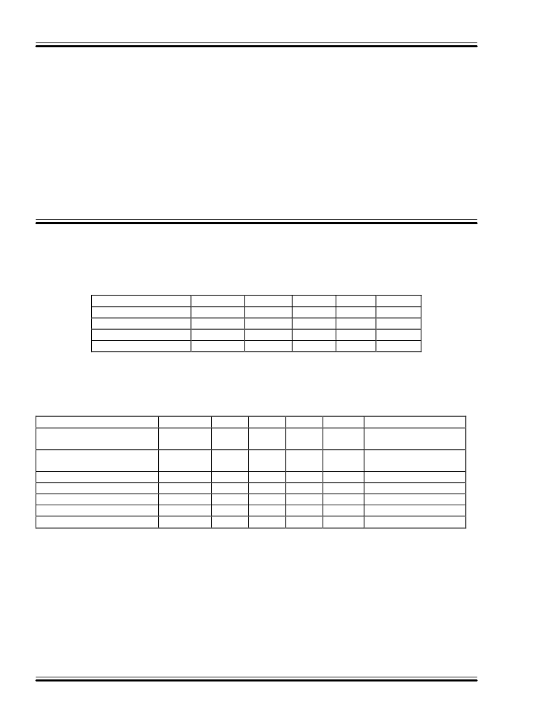
TABLE 1: ABSOLUTE MAXIMUM RATINGS
PARAMETER
DC Supply Voltage
Input Pin Voltage
Storage Temperature
Lead Temperature
SYMBOL
V
DD
V
IN
T
STRG
T
LEAD
MIN
-0.3
-0.3
-55
MAX
7.0
V
DD
+0.3
150
300
UNITS
V
V
C
C
NOTES
10 sec
TABLE 2: DC ELECTRICAL CHARACTERISTICS
(0C to 70C, 4.75V to 5.25V)
PARAMETER
High Level Output Voltage
SYMBOL
V
OH
MIN
3.98
TYP
4.4
MAX
UNITS
V
NOTES
V
DD
= 5.0, I
OH
= MAX
V
IH
= MIN, V
IL
= MAX
V
DD
= 5.0, I
OL
= MAX
V
IH
= MIN, V
IL
= MAX
Low Level Output Voltage
V
OL
0.15
0.26
V
High Level Output Current
Low Level Output Current
High Level Input Voltage
Low Level Input Voltage
Input Current
I
OH
I
OL
V
IH
V
IL
I
IH
-4.0
4.0
mA
mA
V
V
μ
A
3.15
1.35
0.10
V
DD
= 5.0
相關(guān)PDF資料 |
PDF描述 |
|---|---|
| DDU8C-5100M | Delay Line |
| DDU8C-5100MD1 | Delay Line |
| DDU8C-5100MD4 | Delay Line |
| DDU8C-5125 | Tapped Delay Line |
| DDU8C-5125A1 | Delay Line |
相關(guān)代理商/技術(shù)參數(shù) |
參數(shù)描述 |
|---|---|
| DDU8C-5100M | 制造商:未知廠家 制造商全稱:未知廠家 功能描述:Delay Line |
| DDU8C-5100MD1 | 制造商:未知廠家 制造商全稱:未知廠家 功能描述:Delay Line |
| DDU8C-5100MD4 | 制造商:未知廠家 制造商全稱:未知廠家 功能描述:Delay Line |
| DDU8C-5125 | 制造商:DATADELAY 制造商全稱:Data Delay Devices, Inc. 功能描述:5-TAP, HCMOS-INTERFACED FIXED DELAY LINE |
| DDU8C-5125A1 | 制造商:未知廠家 制造商全稱:未知廠家 功能描述:Delay Line |
發(fā)布緊急采購,3分鐘左右您將得到回復(fù)。