- 您現(xiàn)在的位置:買賣IC網(wǎng) > PDF目錄376887 > DR-11800D4-804W Converter PDF資料下載
參數(shù)資料
| 型號: | DR-11800D4-804W |
| 英文描述: | Converter |
| 中文描述: | 轉(zhuǎn)換器 |
| 文件頁數(shù): | 2/4頁 |
| 文件大小: | 87K |
| 代理商: | DR-11800D4-804W |

FIGURE 2. LL, LM, LA TIMING DIAGRAM
2
INTRODUCTION
As shown in FIGURE 1, the signal conversion in the DR-11525 is
performed by a high-accuracy digital-to-resolver converter whose
sin and cos outputs have a low scale factor variation as a func-
tion of the digital input angle.This resolver output is amplified by
scaling amplifiers for resolver output.The output line currents can
be 2 mA rms max, which is sufficient for driving R/D converters,
solid-state control transformers, and displays. Output power
amplifiers will be required, however, for driving electromechanical
devices such as synchros and resolvers.
The reference conditioner has a differential input with high ac and
dc common mode rejection, so that a reference isolation trans-
former will seldom be required.There are three sets of reference
inputs which provide three different input/output ratios. The RH-
RL input provides a 0.45 ratio between the reference input and
the signal output and is designed to provide 11.8 V
L
-
L
differential
output for a 26 Vrms reference input. The RH2-RL2 input pro-
vides a 0.52 ratio between the reference input and the signal out-
put and is designed to provide a 6.81 Vrms single-ended output
for a 26 Vrms reference input. The RH3-RL3 input provides a
0.91 ratio between the reference input and the signal output and
is designed to provide a 2 Vrms single-ended output for a 4.4
Vrms reference input. Series resistors can be added to accom-
modate higher reference levels or to reduce the output level.
The reference conditioner output -R is intended for test purpos-
es. For a 26 Vrms nominal input to RH, RL, -R should be 5.9
Vrms.
The timing relationship of LL, LM, and LA is shown in FIGURE 2
as a design reference.
OUTPUT SCALING AND REF. LEVEL ADJUSTMENT
The DR-11525 operates like a multiplying D/A converter in that
the voltage of each output line is directly proportional to the ref-
erence voltage. Reference FIGURE 3.
The magnitude of the resistors, R', in ohms is calculated as fol-
lows:
For RH-RL: V
OUTL
-
L
45.38k
V
IN
100k + R'
DATA 1-16 BITS
200 ns MIN
LATCHED
TRANSPARENT
100 ns MIN
50 ns MIN
Notes: 1) Maximum reference input RH-RL = 26 V +10%; RH2-RL2 = 26 V +10%;
RH3-RL3 = 16.4 V.
2) Minumum voltage output (when using scalable reference input) is 1 V
differential or 0.5 V single ended.
3) Differential is line-to-line (L-L); single ended is line-to-ground (L-gnd).
=
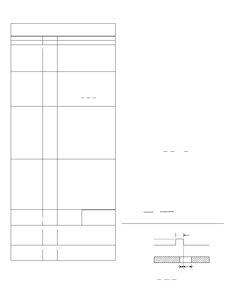
TABLE 1. DR-11525 SPECIFICATIONS
Apply over temperature range, power supply range, reference voltage and
frequency range, and 10% harmonic distortion in the reference.
PARAMETER
UNIT
Bits
RESOLUTION
ACCURACY and
Output Accuracy
VALUE
16
Natural binary angle, parallel positive
logic CMOS and TTL compatible.
Inputs are CMOS transient protected.
Logic 0 = 0 to +1 V
Logic 1 = +2.2 V to +5 V
20 max to GND (bits 1-16)
20 max to +5 V (LL, LM, LA)
See Timing Diagram (FIGURE 2.).
μ
A
DIGITAL INPUT
Logic Type
Load Current
REFERENCE INPUT
Type
Frequency Range
Standard Input
Voltage
(Note 1)
RH3-RL3
RH2-RL2
RH-RL
Input Impedance
Single-Ended:RH-gnd
Differential: RH to RL
ANALOG OUTPUT
Type
Output Current
Standard Output
Voltage
(Note 2)
RH-RL
RH2-RL2
RH3-RL3
Transform. Ratio Tol.
Scale Factor Variation
DC Offset
Single ended
Hz
V
V
V
k ohm
k ohm
Resolver
2 max
(Tracks Reference Input Voltage)
11.8 nominal
6.81 (single ended)
2.0 nominal (single ended)
±0.5 max
±0.1 max
±15 max Varies with input angle.
mA rms
Vrms
L-L
Vrms
Vrms
%
%
mV
V
mAmax
-15 ±5%
-18 V
35+ load current
-55 to +125
0 to +70
-55 to +135
°C
°C
°C
Operation
-1 Option
-3 Option
Storage
PHYSICAL CHARACTERISTICS
Type
Size
Weight
in.(mm)
oz (g)
36 pin DDIP
0.78 x 1.9 x 0.21 (19.7 x 48.1 x 5.3)
0.85 (24)
±4 to ±1 min. (See Ordering info.)
1 minute part: 1 min up to 1 kHz, 1.5 min
for 1 to 5 kHz, and 3 min for 5 to 10 kHz
(guaranteed by design - tested at 5 kHz)
±1 max
Less than 20 for any digital step change
Minutes
LSB
μ
sec
Three differential solid-state inputs: two
for standard 26 V, one programmable.
DC to 10 k
4.4
26
26
100 ±0.5%
200 ±0.5%
+15 ±5%
+18 V
35+ load current
POWER SUPPLIES
Voltage
Max voltage without damage
Current or Impedance
TEMPERATURE RANGES (CASE)
Differential Linearity
Output Setting Time
DYNAMICS
相關(guān)PDF資料 |
PDF描述 |
|---|---|
| DR-11800D4-804Y | Converter |
| DR-11800D4-804Z | Converter |
| DR-11800D4-805 | Converter |
| DR-11800D4-805K | Converter |
| DR-11800D4-805L | Converter |
相關(guān)代理商/技術(shù)參數(shù) |
參數(shù)描述 |
|---|---|
| DR-11800D4-804Y | 制造商:未知廠家 制造商全稱:未知廠家 功能描述:Converter |
| DR-11800D4-804Z | 制造商:未知廠家 制造商全稱:未知廠家 功能描述:Converter |
| DR-11800D4-805 | 制造商:未知廠家 制造商全稱:未知廠家 功能描述:Converter |
| DR-11800D4-805K | 制造商:未知廠家 制造商全稱:未知廠家 功能描述:Converter |
| DR-11800D4-805L | 制造商:未知廠家 制造商全稱:未知廠家 功能描述:Converter |
發(fā)布緊急采購,3分鐘左右您將得到回復(fù)。