- 您現(xiàn)在的位置:買賣IC網(wǎng) > PDF目錄171224 > DS1691A (National Semiconductor Corporation) (RS-422/RS-423) Line Drivers with TRI-STATE Outputs((RS-422/RS-423) 三態(tài)輸出的線驅(qū)動(dòng)器) PDF資料下載
參數(shù)資料
| 型號: | DS1691A |
| 廠商: | National Semiconductor Corporation |
| 英文描述: | (RS-422/RS-423) Line Drivers with TRI-STATE Outputs((RS-422/RS-423) 三態(tài)輸出的線驅(qū)動(dòng)器) |
| 中文描述: | (RS-422/RS-423)線路驅(qū)動(dòng)器,三態(tài)輸出((RS-422/RS-423)三態(tài)輸出的線驅(qū)動(dòng)器) |
| 文件頁數(shù): | 4/10頁 |
| 文件大小: | 275K |
| 代理商: | DS1691A |
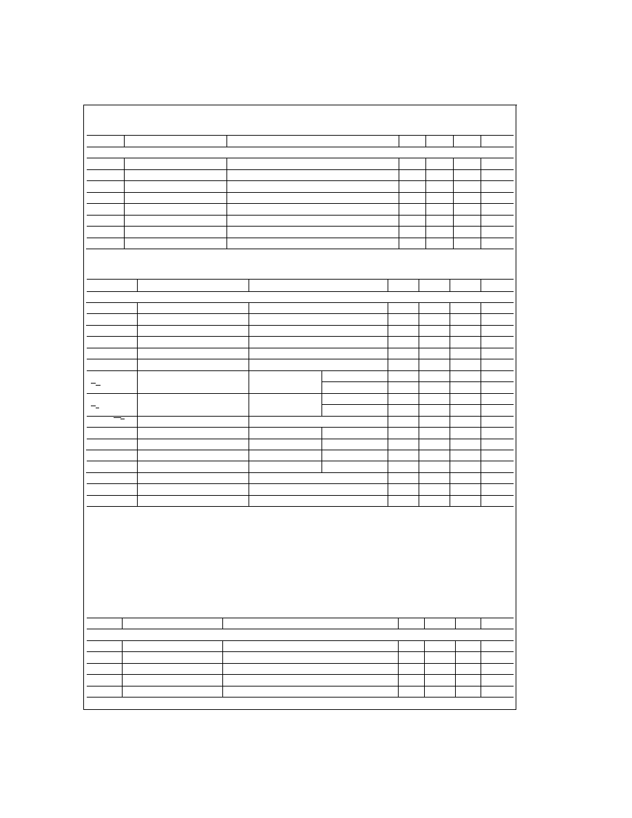
AC Electrical Characteristics (Note 6)
T
A = 25C
Symbol
Parameter
Conditions
Min
Typ
Max
Units
RS-422 CONNECTION, V
CC = 5V, MODE SELECT = 0.8V
t
r
Output Rise Time
R
L = 100,CL = 500 pF (Figure 1 )
120
200
ns
t
f
Output Fall Time
R
L = 100,CL = 500 pF (Figure 1 )
120
200
ns
t
PDH
Output Propagation Delay
R
L = 100,CL = 500 pF (Figure 1 )
120
200
ns
t
PDL
Output Propagation Delay
R
L = 100,CL = 500 pF (Figure 1 )
120
200
ns
t
PZL
TRI-STATE Delay
R
L = 450,CL = 500 pF, CC = 0pF (Figure 4 )
250
350
ns
t
PZH
TRI-STATE Delay
R
L = 450,CL = 500 pF, CC = 0pF (Figure 4 )
180
300
ns
t
PLZ
TRI-STATE Delay
R
L = 450,CL = 500 pF, CC = 0pF (Figure 4 )
180
300
ns
t
PHZ
TRI-STATE Delay
R
L = 450,CL = 500 pF, CC = 0pF (Figure 4 )
250
350
ns
DC Electrical Characteristics (Notes 3, 4, 5, 6)
Symbol
Parameter
Conditions
Min
Typ
Max
Units
RS-423 CONNECTION, |V
CC| = |V EE|, MODE SELECT ≥ 2V
V
IH
High Level Input Voltage
2
V
IL
Low Level Input Voltage
0.8
V
I
IH
High Level Input Current
V
IN = 2.4V
1
40
A
V
IN ≤ 15V
10
100
A
I
IL
Low Level Input Current
V
IN = 0.4V
30
200
A
V
I
Input Clamp Voltage
I
IN = 12 mA
1.5
V
O
Output Voltage
R
L = ∞, (Note 7)
V
IN = 2V
4.0
4.4
6.0
V
O
V
CC ≥ 4.75V
V
IN = 0.4V
4.0
4.4
6.0
V
T
Output Voltage
R
L = 450
V
IN = 2.4V
3.6
4.1
V
T
V
CC ≥ 4.75V
V
IN = 0.4V
3.6
4.1
V
|V
T||VT |
Output Unbalance
|V
CC| = |VEE| = 4.75V, R L = 450
0.02
0.4
V
I
X
+
Output Leakage Power OFF
V
CC = V EE = 0V
V
O = 6V
2
100
A
I
X
Output Leakage Power OFF
V
CC = V EE = 0V
V
O = 6V
2
100
A
I
S
+
Output Short Circuit Current
V
O = 0V
V
IN = 2.4V
80
150
mA
I
S
Output Short Circuit Current
V
O = 0V
V
IN = 0.4V
80
150
mA
I
SLEW
Slew Control Current
±140
A
I
CC
Positive Supply Current
V
IN = 0.4V, RL = ∞
18
30
mA
I
EE
Negative Supply Current
V
IN = 0.4V, RL = ∞
10
22
mA
Note 2: “Absolute Maximum Ratings” are those values beyond which the safety of the device cannot be guaranteed. They are not meant to imply that the devices
should be operated at these limits. The tables of “Electrical Characteristics” provide conditions for actual device operation.
Note 3: Unless otherwise specified, min/max limits apply across the 55C to +125C temperature range for the DS1691A and across the 0C to +70C range for
the DS3691. All typicals are given for V CC = 5V and TA = 25C. VCC and VEE as listed in operating conditions.
Note 4: All currents into device pins are positive; all currents out of device pins are negative. All voltages are referenced to ground unless otherwise specified.
Note 5: Only one output at a time should be shorted.
Note 6: Symbols and definitions correspond to EIA RS-422 and/or RS-423 where applicable.
Note 7: At 55C, the output voltage is +3.9V minimum and 3.9V minimum.
AC Electrical Characteristics (Note 6)
T
A = 25C
Symbol
Parameter
Conditions
Min
Typ
Max
Units
RS-423 CONNECTION, V
CC = 5V, VEE 5V, MODE SELECT = 2.4V
t
r
Rise Time
R
L = 450,CL = 500 pF, CC = 0(Figure 2 )
120
300
ns
t
f
Fall Time
R
L = 450,CL = 500 pF, CC = 0(Figure 2 )
120
300
ns
t
r
Rise Time
R
L = 450,CL = 500 pF CC = 50 pF (Figure 3 )
3.0
s
t
f
Fall Time
R
L = 450,CL = 500 pF CC = 50 pF (Figure 3 )
3.0
s
t
rc
Rise Time Coefficient
R
L = 450,CL = 500 pF, CC = 50 pF (Figure 3 )
0.06
s/pF
3
www.national.com
相關(guān)PDF資料 |
PDF描述 |
|---|---|
| DS1812Z-5 | 1-CHANNEL POWER SUPPLY SUPPORT CKT, PDSO3 |
| DS1813R-10T&R | 1-CHANNEL POWER SUPPLY SUPPORT CKT, PDSO3 |
| DS1819AR-5T&R | 1-CHANNEL POWER SUPPLY MANAGEMENT CKT, PDSO5 |
| DS1814AR-10 | 1-CHANNEL POWER SUPPLY MANAGEMENT CKT, PDSO5 |
| DS1819CR-10T&R | 1-CHANNEL POWER SUPPLY SUPPORT CKT, PDSO5 |
相關(guān)代理商/技術(shù)參數(shù) |
參數(shù)描述 |
|---|---|
| DS1691AJ/883 | 制造商:NSC 制造商全稱:National Semiconductor 功能描述:(RS-422/RS-423) Line Drivers with TRI-STATE Outputs |
| DS1691AJ/A+ | 制造商:未知廠家 制造商全稱:未知廠家 功能描述:Line Driver |
| DS1691J | 制造商:未知廠家 制造商全稱:未知廠家 功能描述:Line Driver |
| DS1692 | 制造商:NSC 制造商全稱:National Semiconductor 功能描述:TRI-STATE Differential Line Drivers |
| DS1692J | 制造商:Maxim Integrated Products 功能描述: |
發(fā)布緊急采購,3分鐘左右您將得到回復(fù)。