- 您現(xiàn)在的位置:買賣IC網(wǎng) > PDF目錄1914 > DS2106S/T&R (Maxim Integrated Products)IC TERMINATOR SCSI 28-SOIC PDF資料下載
參數(shù)資料
| 型號: | DS2106S/T&R |
| 廠商: | Maxim Integrated Products |
| 文件頁數(shù): | 2/6頁 |
| 文件大小: | 0K |
| 描述: | IC TERMINATOR SCSI 28-SOIC |
| 標(biāo)準(zhǔn)包裝: | 1,000 |
| 安裝類型: | 表面貼裝 |
| 供應(yīng)商設(shè)備封裝: | 28-SOIC |
| 包裝: | 帶卷 (TR) |

DS2106
022698 2/6
REFERENCE DOCUMENTS
SCSI–2 (X3.131–1994)
SCSI–3 Parallel Interface (X3T10/855D)
SCSI–3 Fast–20 (X3T10/1071D)
Available from: Global Engineering Documents
15 Inverness Way East
Englewood, CO 80112–5704
Phone: (800) 854–7179,(303) 792–2181
Fax: (303) 792–2192
FUNCTION DESCRIPTION
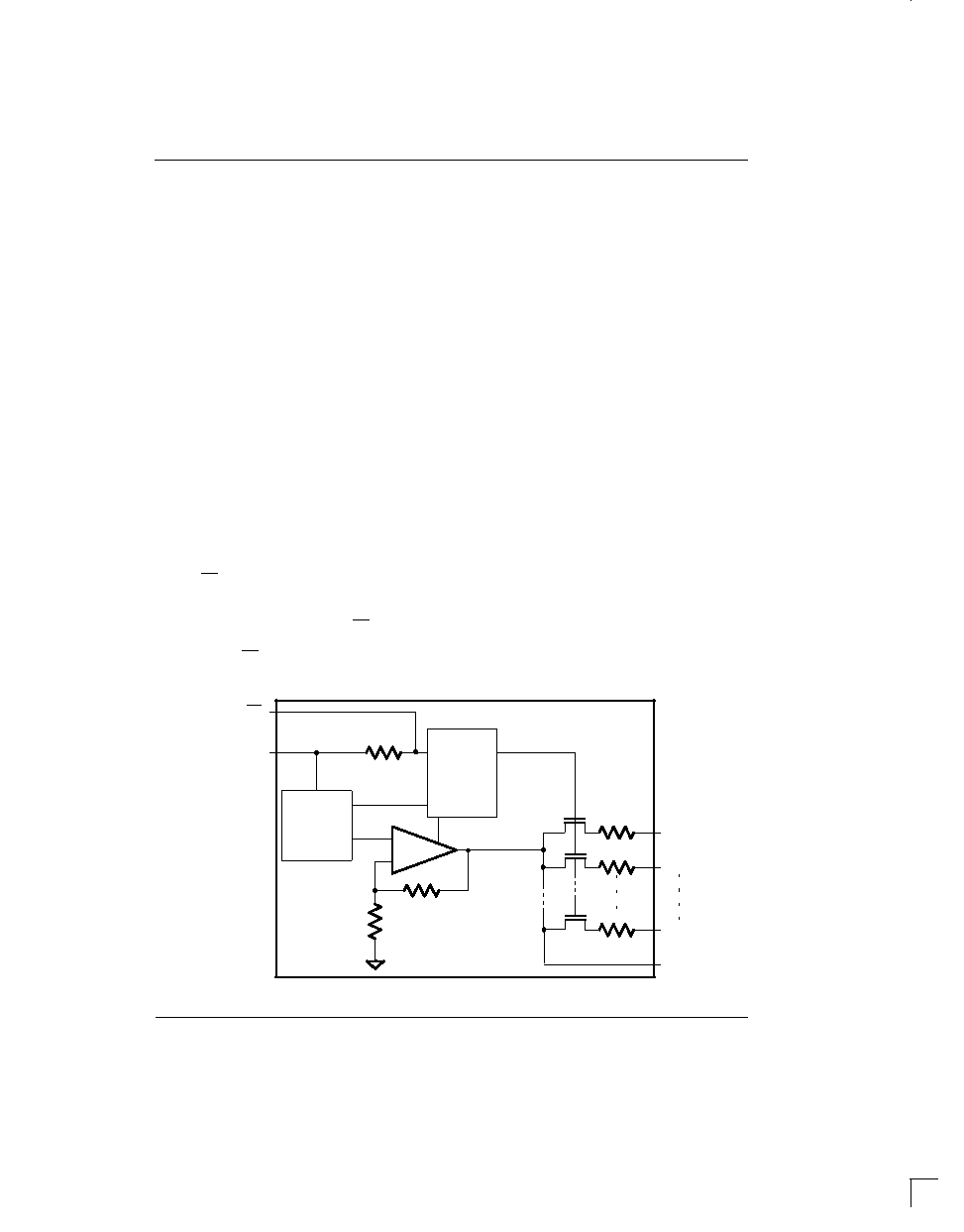
The DS2106 is designed to be a single chip termination
subsystem for use in Narrow SCSI systems.
The
DS2106 consists of a bandgap reference, buffer ampli-
fier, and 18 termination resistors (Figure 1). The voltage
regulator circuitry (bandgap reference and class AB
power amplifier) produces a precise laser trimmed 2.85
volt level and is capable of sourcing 24 mA into each of
the terminating resistors when the signal line is low
(active). When the external driver for a given signal line
turns off, the active terminator will pull that signal line to
2.85 volts (quiescent state). When used with an active
negation driver, the power amp can sink 22 mA per line
while keeping the voltage reference in regulation; the
terminating resistors maintain their 110 ohm value over
the entire voltage range. When all lines settle in the
quiescent state, the regulator will consume about
10 mA.
When the DS2106 is put into power–down mode by
bringing PD low, the power–down circuitry will turn off
the transistors on each signal line. This will isolate the
DS2106 from the signal lines and effectively remove it
from the circuit. The power–down pin (PD) has an inter-
nal 50K
pull–up resistor. To place the DS2106 into an
active state, the PD pin should be left open circuited.
To ensure proper operation, the TPWR pin should be
connected to the SCSI bus TERMPWR line. As with all
analog circuitry, the TERMPWR lines should be
bypassed locally. A 2.2
F capacitor and a 0.01 F high
frequency capacitor is recommended between TPWR
and ground and placed as close as possible to the
DS2106. The DS2106 should be placed as close as
possible to the connector to minimize signal and power
trace length, thereby resulting in less input capacitance
and reflections which can degrade the bus signals.
To maintain the specified regulation, a 4.7
F capacitor
is required between the VREF pin and ground of each
DS2106. A high frequency cap (0.1
F ceramic recom-
mended) can also be placed on the VREF pin in applica-
tions that use fast rise/fall time drivers. Figure 2 details a
typical SCSI bus configuration. In an 8–bit data SCSI
bus (Narrow SCSI), one DS2106 is needed for proper
termination of the 18 active signal lines. One DS2106
and one DS21S07A can be used to terminate the 27
active signal lines in a 16–bit data SCSI bus (Wide
SCSI).
DS2106 BLOCK DIAGRAM Figure 1
PD
POWER
DOWN
CIRCUIT-
RY
50K ohm
BANDGAP
REFERENCE
R18
R17
R1
VREF
110 ohms
+
–
TPWR
相關(guān)PDF資料 |
PDF描述 |
|---|---|
| DS2108S+T&R | IC TERM SCSI DIFF/SWITCH 24-SOIC |
| DS2114Z | IC TERM SCSI 2% 150MIL 16-SOIC |
| DS2117MX/T&R | IC TERM SCSI LVD/SE ULT-3 FCHIP |
| DS2118MB+T&R | IC TERM SCSI LVD/SE ULT-3 36SSOP |
| DS2119ME+T&R | IC TERM SCSI LVD/SE ULT3 28TSSOP |
相關(guān)代理商/技術(shù)參數(shù) |
參數(shù)描述 |
|---|---|
| DS2106SV32 | 制造商:Dynex Semiconductor 功能描述:RECTIFIER MODULE - STANDARD RECOVERY |
| DS2106SY | 制造商:DYNEX 制造商全稱:Dynex Semiconductor 功能描述:Rectifier Diode |
| DS2106SY35 | 制造商:Dynex Semiconductor 功能描述:RECTIFIER MODULE - STANDARD RECOVERY |
| DS2106SY36 | 制造商:Dynex Semiconductor 功能描述:RECTIFIER MODULE - STANDARD RECOVERY |
| DS2106SY37 | 制造商:DYNEX 制造商全稱:Dynex Semiconductor 功能描述:Rectifier Diode |
發(fā)布緊急采購,3分鐘左右您將得到回復(fù)。