- 您現(xiàn)在的位置:買賣IC網(wǎng) > PDF目錄376982 > DS8187 PDF資料下載
參數(shù)資料
| 型號: | DS8187 |
| 文件頁數(shù): | 5/12頁 |
| 文件大小: | 196K |
| 代理商: | DS8187 |
Functional Description
SHIFT REGISTER OPERATION
Refer to block diagram Figure 1 while LOAD ENABLE is
low, data is entered into the shift register on the rising edge
of the clock. The first data bit entered is stored in position
Y
0, the last data bit entered is stored in position
Y
33. A
high voltage level applied to the LOAD ENABLE input trans-
fers the data from the shift register to the data latch. The
data is presented to the output drivers through a 33 x 33
matrix. This matrix determines shift register output designa-
tion. The DS8187 has 34 shift register positions, 33 data
latches, and 33 output drivers.
AUTO LOAD MODE
In this mode, the DATA OUT pin is connected to the LOAD
ENABLE pin. The data word consists of 34 bits including a
leading start bit(logic 1). On the positive-going-edge of the
34th clock (LOAD ENABLE goes High), data is transferred
to the data latches and the shift register is cleared.
DIRECT LOAD MODE
In this mode the DATA OUT pin is not connected to the
LOAD ENABLE pin. The LOAD ENABLE pin is controlled
directly by the user. When LOAD ENABLE goes High, the
contents of the shift register are latched, presented to the
output drivers through the 33 x 33 PLA matrix, and the shift
register is cleared.
DIMMING FUNCTION
When VK is Low, the BLANK IN/PWM OUT pin functions as
an input blanking signal. When BLANK IN/PWM is High, the
output duty cycle is 100%. The duty cycle of a user supplied
signal to this pin will determine the brightness of the output.
When VK is High, the duty cycle of the output drivers is
controlled by an analog voltage applied to the VD pin.
Table I indicates the duty cycle of the output drivers with
respect to the analog voltage applied to VD pin.
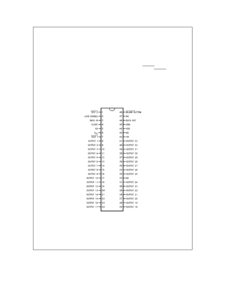
Connection Diagram
Dual-In-Line Package
TL/F/11220–1
Top View
Order Number DS8187N
See NS Package Number N48A
5
相關PDF資料 |
PDF描述 |
|---|---|
| DS850-3 | 850 Watts 12V |
| DS850-9 | 850 Watts 48V Distributed Power System |
| DS8617 | |
| DS8617M-4 | Prescaler/Frequency Divider |
| DS8617N-2 | Prescaler/Frequency Divider |
相關代理商/技術參數(shù) |
參數(shù)描述 |
|---|---|
| DS819 | 制造商:未知廠家 制造商全稱:未知廠家 功能描述:Analog IC |
| DS830 | 制造商:未知廠家 制造商全稱:未知廠家 功能描述:Analog IC |
| DS8313 | 制造商:MAXIM 制造商全稱:Maxim Integrated Products 功能描述:Smart Card Interface |
| DS8313+RJX | 制造商:Maxim Integrated Products 功能描述:- Rail/Tube |
| DS8313+RRX | 制造商:Maxim Integrated Products 功能描述:- Rail/Tube |
發(fā)布緊急采購,3分鐘左右您將得到回復。