- 您現(xiàn)在的位置:買賣IC網(wǎng) > PDF目錄376985 > DS90LV032ATMTCX Line Receiver PDF資料下載
參數(shù)資料
| 型號(hào): | DS90LV032ATMTCX |
| 元件分類: | 接收器 |
| 英文描述: | Line Receiver |
| 中文描述: | 線路接收器 |
| 文件頁(yè)數(shù): | 4/8頁(yè) |
| 文件大小: | 162K |
| 代理商: | DS90LV032ATMTCX |

Parameter Measurement Information
(Continued)
Typical Application
Applications Information
General application guidelines and hints for LVDS drivers
and receivers may be found in the following application
notes: LVDS Owner’s Manual (lit #550062-002), AN-808,
AN-977, AN-971, AN-916, AN-805, AN-903.
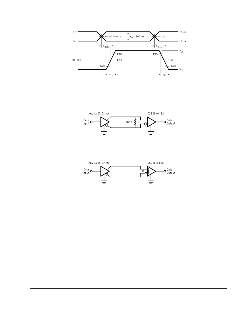
LVDS drivers and receivers are intended to be primarily used
in an uncomplicated point-to-point configuration as is shown
in
Figure 3
. This configuration provides a clean signaling
environment for the fast edge rates of the drivers. The re-
ceiver is connected to the driver through a balanced media
which may be a standard twisted pair cable, a parallel pair
cable, or simply PCB traces. Typically the characteristic
impedance of the media is in the range of 100
. A termina-
tion resistor of 100
should be selected to match the media,
and is located as close to the receiver input pins as possible.
The termination resistor converts the driver output (current
mode) into a voltage that is detected by the receiver. Other
configurations are possible such as a multi-receiver configu-
ration, but the effects of a mid-stream connector(s), cable
stub(s), and other impedance discontinuities as well as
ground shifting, noise margin limits, and total termination
loading must be taken into account.
The DS90LV012A and DS90LT012A differential line receiv-
ers are capable of detecting signals as low as 100 mV, over
a
±
1V common-mode range centered around +1.2V. This is
related to the driver offset voltage which is typically +1.2V.
The driven signal is centered around this voltage and may
shift
±
1V around this center point. The
±
1V shifting may be
the result of a ground potential difference between the driv-
er’s ground reference and the receiver’s ground reference,
the common-mode effects of coupled noise, or a combina-
tion of the two. The AC parameters of both receiver input
pins are optimized for a recommended operating input volt-
age range of 0V to +2.4V (measured from each pin to
ground). The device will operate for receiver input voltages
up to V
, but exceeding V
will turn on the ESD protection
circuitry which will clamp the bus voltages.
20015004
FIGURE 2. Receiver Propagation Delay and Transition Time Waveforms
Balanced System
20015005
FIGURE 3. Point-to-Point Application (DS90LV012A)
Balanced System
20015028
FIGURE 4. Point-to-Point Application (DS90LT012A)
D
www.national.com
4
相關(guān)PDF資料 |
PDF描述 |
|---|---|
| DS90LV032ATMX | Line Receiver |
| DS90LV047ATMTCX | Line Driver |
| DS90LV047ATMX | Line Driver |
| DS90LV048ATMTCX | Line Receiver |
| DS90LV048ATMX | Line Receiver |
相關(guān)代理商/技術(shù)參數(shù) |
參數(shù)描述 |
|---|---|
| DS90LV032ATMTCX/NOPB | 功能描述:LVDS 接口集成電路 RoHS:否 制造商:Texas Instruments 激勵(lì)器數(shù)量:4 接收機(jī)數(shù)量:4 數(shù)據(jù)速率:155.5 Mbps 工作電源電壓:5 V 最大功率耗散:1025 mW 最大工作溫度:+ 85 C 封裝 / 箱體:SOIC-16 Narrow 封裝:Reel |
| DS90LV032ATMX | 功能描述:LVDS 接口集成電路 RoHS:否 制造商:Texas Instruments 激勵(lì)器數(shù)量:4 接收機(jī)數(shù)量:4 數(shù)據(jù)速率:155.5 Mbps 工作電源電壓:5 V 最大功率耗散:1025 mW 最大工作溫度:+ 85 C 封裝 / 箱體:SOIC-16 Narrow 封裝:Reel |
| DS90LV032ATMX/NOPB | 功能描述:LVDS 接口集成電路 RoHS:否 制造商:Texas Instruments 激勵(lì)器數(shù)量:4 接收機(jī)數(shù)量:4 數(shù)據(jù)速率:155.5 Mbps 工作電源電壓:5 V 最大功率耗散:1025 mW 最大工作溫度:+ 85 C 封裝 / 箱體:SOIC-16 Narrow 封裝:Reel |
| DS90LV032AWGMLS | 功能描述:LVDS 接口集成電路 RoHS:否 制造商:Texas Instruments 激勵(lì)器數(shù)量:4 接收機(jī)數(shù)量:4 數(shù)據(jù)速率:155.5 Mbps 工作電源電壓:5 V 最大功率耗散:1025 mW 最大工作溫度:+ 85 C 封裝 / 箱體:SOIC-16 Narrow 封裝:Reel |
| DS90LV032AWGMPR | 制造商:Texas Instruments 功能描述: |
發(fā)布緊急采購(gòu),3分鐘左右您將得到回復(fù)。