- 您現(xiàn)在的位置:買賣IC網(wǎng) > PDF目錄295863 > DXT3150-13 (DIODES INC) PDF資料下載
參數(shù)資料
| 型號: | DXT3150-13 |
| 廠商: | DIODES INC |
| 元件分類: | 小信號晶體管 |
| 中文描述: | 5 mA, 25 V, NPN, Si, SMALL SIGNAL TRANSISTOR |
| 封裝: | GREEEN, PLASTIC, SOT89-3L, 4 PIN |
| 文件頁數(shù): | 1/3頁 |
| 文件大小: | 199K |
| 代理商: | DXT3150-13 |
DXT3150
NPN SURFACE MOUNT TRANSISTOR
Features
Epitaxial Planar Die Construction
Ideally Suited for Automated Assembly Processes
Ideal for Medium Power Switching or Amplification Applications
Lead Free By Design/RoHS Compliant (Note 1)
"Green" Device (Note 2)
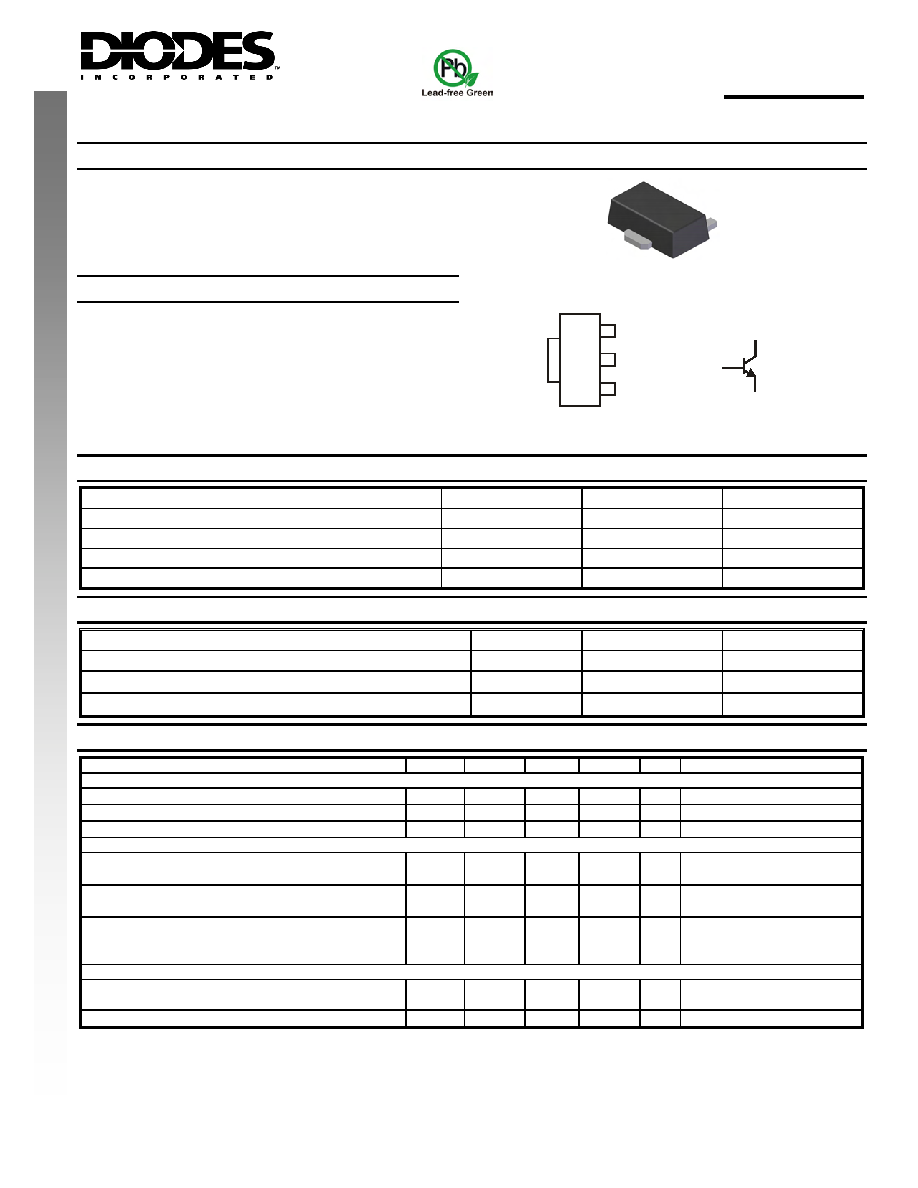
Mechanical Data
Case: SOT89-3L
Case Material: Molded Plastic, “Green” Molding Compound.
UL Flammability Classification Rating 94V-0
Moisture Sensitivity: Level 1 per J-STD-020C
Terminals: Finish — Matte Tin annealed over Copper leadframe
(Lead Free Plating). Solderable per MIL-STD-202, Method 208
Marking & Type Code Information: See Page 3
Ordering Information: See Page 3
Weight: 0.072 grams (approximate)
NEW
PROD
UC
T
SOT89-3L
3
1
2,4
COLLECTOR
EMITTER
BASE
4
3
2
1
C
B
E
TOP VIEW
Schematic and Pin Configuration
Maximum Ratings @TA = 25°C unless otherwise specified
Characteristic
Symbol
Value
Unit
Collector-Base Voltage
VCBO
50
V
Collector-Emitter Voltage
VCEO
25
V
Emitter-Base Voltage
VEBO
7
V
Continuous Collector Current
IC
5
A
Thermal Characteristics
Characteristic
Symbol
Value
Unit
Power Dissipation (Note 3) @ TA = 25°C
PD
1
W
Thermal Resistance, Junction to Ambient Air (Note 3) @TA = 25°C
RθJA
125
°C/W
Operating and Storage Temperature Range
Tj, TSTG
-55 to +150
°C
Electrical Characteristics @TA = 25°C unless otherwise specified
Characteristic
Symbol
Min
Typ
Max
Unit
Test Conditions
OFF CHARACTERISTICS (Note 4)
Collector-Emitter Breakdown Voltage
V(BR)CEO
25
V
IC = 10mA, IB = 0
Collector Cut-off Current
ICBO
1.0
μA
VCB = 50V, IE = 0
Emitter Cut-off Current
IEBO
1.0
μA
VEB = 7.0V, IC = 0
ON CHARACTERISTICS (Note 4)
Collector-Emitter Saturation Voltage
VCE(SAT)
0.35
0.50
V
IC = 3.0A, IB = 150mA
IC = 4.0A, IB = 200mA
Base-Emitter Saturation Voltage
VBE(SAT)
1.10
1.40
V
IC = 3.0A, IB = 150mA
IC = 4.0A, IB = 200mA
DC Current Gain
hFE
250
150
50
550
IC = 500mA, VCE = 2.0V
IC = 2.0A, VCE = 2.0V
IC = 5.0A, VCE = 2.0V
SMALL SIGNAL CHARACTERISTICS
Current Gain-Bandwidth Product
fT
220
MHz
IC = 50mA, VCE = 6.0V,
f = 100MHz
Output Capacitance
Cobo
50
pF
VCB = 10V, IE = 0, f = 1MHz
Notes:
1.
No purposefully added lead.
2.
Diodes Inc.'s "Green" policy can be found on our website at http://www.diodes.com/products/lead_free/index.php.
3.
Device mounted on FR-4 PCB; pad layout as shown on page 3 or in Diodes Inc. suggested pad layout document AP02001, which can be found on our
website at http://www.diodes.com/datasheets/ap02001.pdf.
4.
Measured under pulsed conditions. Pulse width = 300
μs. Duty cycle ≤2%.
DS31157 Rev. 3 - 2
1 of 3
www.diodes.com
DXT3150
Diodes Incorporated
相關PDF資料 |
PDF描述 |
|---|---|
| DZ33T63 | TIME LAG BLOW ELECTRIC FUSE, 63A, 500VAC, 500VDC, 80000A (IR), INLINE/HOLDER |
| DZ33T50 | TIME LAG BLOW ELECTRIC FUSE, 50A, 500VAC, 500VDC, 80000A (IR), INLINE/HOLDER |
| DZ33T35 | TIME LAG BLOW ELECTRIC FUSE, 35A, 500VAC, 500VDC, 80000A (IR), INLINE/HOLDER |
| DZ33F63 | FAST BLOW ELECTRIC FUSE, 63A, 500VAC, 500VDC, 80000A (IR), INLINE/HOLDER |
| DZ33F50 | FAST BLOW ELECTRIC FUSE, 50A, 500VAC, 500VDC, 80000A (IR), INLINE/HOLDER |
相關代理商/技術(shù)參數(shù) |
參數(shù)描述 |
|---|---|
| DXT3832.768 | 制造商:Alpha 3 Manufacturing 功能描述: |
| DXT3832.768-SLA15 | 制造商:Alpha 3 Manufacturing 功能描述: |
| DXT3904 | 制造商:DIODES 制造商全稱:Diodes Incorporated 功能描述:NPN SURFACE MOUNT TRANSISTOR |
| DXT3904-13 | 功能描述:兩極晶體管 - BJT 1000mW 40Vceo RoHS:否 制造商:STMicroelectronics 配置: 晶體管極性:PNP 集電極—基極電壓 VCBO: 集電極—發(fā)射極最大電壓 VCEO:- 40 V 發(fā)射極 - 基極電壓 VEBO:- 6 V 集電極—射極飽和電壓: 最大直流電集電極電流: 增益帶寬產(chǎn)品fT: 直流集電極/Base Gain hfe Min:100 A 最大工作溫度: 安裝風格:SMD/SMT 封裝 / 箱體:PowerFLAT 2 x 2 |
| DXT3906 | 制造商:DCCOM 制造商全稱:Dc Components 功能描述:TECHNICAL SPECIFICATIONS OF PNP EPITAXIAL PLANAR TRANSISTOR |
發(fā)布緊急采購,3分鐘左右您將得到回復。