- 您現(xiàn)在的位置:買賣IC網(wǎng) > PDF目錄93307 > ECH8603 PDF資料下載
參數(shù)資料
| 型號: | ECH8603 |
| 文件頁數(shù): | 3/4頁 |
| 文件大小: | 33K |
| 代理商: | ECH8603 |
ECH8603
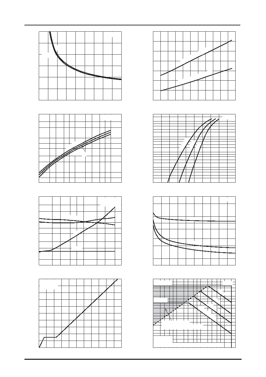
No.7218-3/4
0
4
8
12
16
22
20
2
6
10
14
18
0
--9
--10
--6
--8
--7
--4
--5
--2
--1
--3
VGS -- Qg
IT04375
A S O
--100
--10
2
3
5
7
2
3
5
7
2
3
5
7
2
3
5
7
--1.0
--0.1
--0.01
--1.0
23
5 7
--10
--0.01
--0.1
23
5 7
2
3
5 7
2
3
IT04376
yfs -- ID
IT04371
SW Time -- ID
IT04373
Ciss, Coss, Crss -- VDS
IT04372
--0.001
--0.01
--0.1
--10
--1.0
7
5
3
2
7
5
3
2
7
5
3
2
7
5
3
2
3
2
IF -- VSD
IT04374
10
20
30
40
70
60
50
RDS(on) -- VGS
--60
20
--40
--20
0
20
60
40
80
100
140
120
90
40
70
80
60
50
30
160
IT04369
IT04370
RDS(on) -- Ta
--2
--4
--6
--8
--10
--1
--3
--5
--7
--9
ID= --2A
--1A
Ta=25
°C
ID=
--2A,
VGS
= --4.5V
I D
= --
1A,
V GS
= --
2.5V
T
a=75
°C
25
°C
--25
°C
VGS=0
--0.2
--0.4
--0.6
--0.8
--1.2
--1.1
--1.0
--0.3
--0.5
--0.7
--0.9
IDP= --40A
ID= --4A
100ms
DC
operation
1ms
10ms
<10
s
Operation in this
area is limited by RDS(on).
VDS= --10V
ID= --4A
Total Gate Charge, Qg -- nC
Gate-to-Source
V
oltage,
V
GS
--
V
Drain-to-Source Voltage, VDS -- V
Drain
Current,
I
D
-
A
Ta=25
°C
Single pulse
Mounted on a ceramic board(900mm2!0.8mm)
Drain Current, ID -- A
Switching
T
ime,
SW
T
ime
-
ns
Drain Current, ID -- A
F
orw
ard
T
ransfer
Admittance,
y
fs
-
S
Diode Forward Voltage, VSD -- V
F
orw
ard
Current,
I
F
--
A
Drain-to-Source Voltage, VDS -- V
Ciss,
Coss,
Crss
-
pF
Static
Drain-to-Source
On-State
Resistance,
R
DS
(on)
-
m
Static
Drain-to-Source
On-State
Resistance,
R
DS
(on)
-
m
Gate-to-Source Voltage, VGS -- V
Ambient Temperature, Ta --
°C
0
--2
--4
--6
--8
--10
--12
--14
--16
--18
--20
100
1000
7
5
3
7
2
3
2
Ciss
Crss
Coss
f=1MHz
--0.1
1.0
--10
--1.0
7
5
3
7
5
2
5
3
2
10
7
5
3
27
5
3
22
VDS= --10V
--0.1
--1.0
23
5
7
23
5
7
5
3
2
10
100
7
5
3
2
75°
C
25°
C
Ta=
--25
°C
VDD= --10V
VGS= --4.5V
td(on)
td(off)
tf
t r
相關(guān)PDF資料 |
PDF描述 |
|---|---|
| ECHOCANCELFS | Freescale Semiconductor Digital Network Echo Cancellers |
| ECICM500 | ASIC |
| ECICM600 | ASIC |
| ECICMA | ASIC |
| ECICMB | ASIC |
相關(guān)代理商/技術(shù)參數(shù) |
參數(shù)描述 |
|---|---|
| ECH8603-TL-E | 制造商:SANYO 功能描述:P+P 20V 4A ECH8 Tape & Reel 制造商:SANYO Semiconductor Co Ltd 功能描述:MOSFET PP CH 20V 4A ECH8 制造商:Sanyo 功能描述:0 |
| ECH8604 | 制造商:SANYO 制造商全稱:Sanyo Semicon Device 功能描述:N CHANNEL MOS SILICON TRANSISTOR |
| ECH8604-TL-E | 制造商:SANYO Semiconductor Co Ltd 功能描述:MOSFET N CH 20V 6A ECH8 |
| ECH8605 | 制造商:SANYO 制造商全稱:Sanyo Semicon Device 功能描述:Ultrahigh-Speed Switching Applications |
| ECH8605-TL-E | 制造商:SANYO Semiconductor Co Ltd 功能描述:Cut Tape |
發(fā)布緊急采購,3分鐘左右您將得到回復(fù)。