- 您現(xiàn)在的位置:買(mǎi)賣(mài)IC網(wǎng) > PDF目錄384279 > EDE1104ABSE-8E-E (ELPIDA MEMORY INC) 1G bits DDR2 SDRAM PDF資料下載
參數(shù)資料
| 型號(hào): | EDE1104ABSE-8E-E |
| 廠商: | ELPIDA MEMORY INC |
| 元件分類: | DRAM |
| 英文描述: | 1G bits DDR2 SDRAM |
| 中文描述: | 256M X 4 DDR DRAM, 0.4 ns, PBGA68 |
| 封裝: | ROHS COMPLIANT, FBGA-68 |
| 文件頁(yè)數(shù): | 32/82頁(yè) |
| 文件大?。?/td> | 618K |
| 代理商: | EDE1104ABSE-8E-E |
第1頁(yè)第2頁(yè)第3頁(yè)第4頁(yè)第5頁(yè)第6頁(yè)第7頁(yè)第8頁(yè)第9頁(yè)第10頁(yè)第11頁(yè)第12頁(yè)第13頁(yè)第14頁(yè)第15頁(yè)第16頁(yè)第17頁(yè)第18頁(yè)第19頁(yè)第20頁(yè)第21頁(yè)第22頁(yè)第23頁(yè)第24頁(yè)第25頁(yè)第26頁(yè)第27頁(yè)第28頁(yè)第29頁(yè)第30頁(yè)第31頁(yè)當(dāng)前第32頁(yè)第33頁(yè)第34頁(yè)第35頁(yè)第36頁(yè)第37頁(yè)第38頁(yè)第39頁(yè)第40頁(yè)第41頁(yè)第42頁(yè)第43頁(yè)第44頁(yè)第45頁(yè)第46頁(yè)第47頁(yè)第48頁(yè)第49頁(yè)第50頁(yè)第51頁(yè)第52頁(yè)第53頁(yè)第54頁(yè)第55頁(yè)第56頁(yè)第57頁(yè)第58頁(yè)第59頁(yè)第60頁(yè)第61頁(yè)第62頁(yè)第63頁(yè)第64頁(yè)第65頁(yè)第66頁(yè)第67頁(yè)第68頁(yè)第69頁(yè)第70頁(yè)第71頁(yè)第72頁(yè)第73頁(yè)第74頁(yè)第75頁(yè)第76頁(yè)第77頁(yè)第78頁(yè)第79頁(yè)第80頁(yè)第81頁(yè)第82頁(yè)
EDE1104ABSE, EDE1108ABSE, EDE1116ABSE
Data Sheet E0852E50 (Ver. 5.0)
32
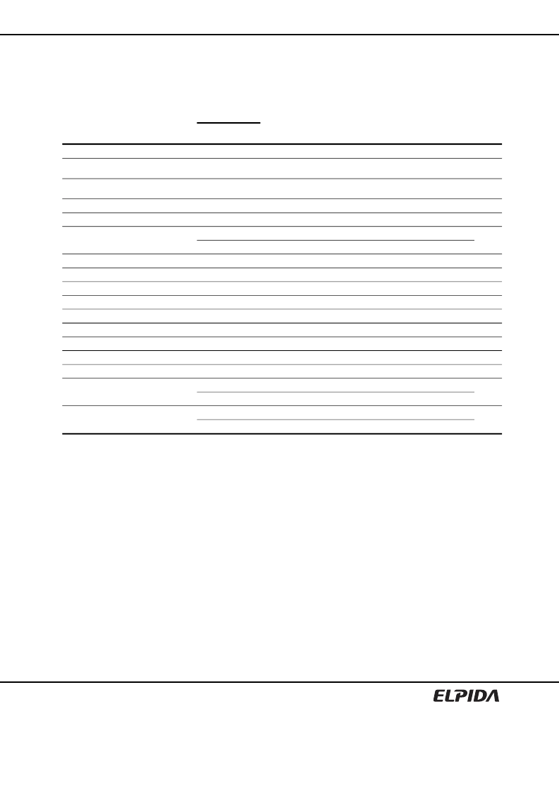
Command Operation
Command Truth Table
The DDR2 SDRAM recognizes the following commands specified by the /CS, /RAS, /CAS, /WE and address pins.
CKE
Function
Symbol
Previous
cycle
Current
cycle
/CS
/RAS
/CAS
/WE BA0 BA1 BA2
A13 to
A11
A10
A0 to
A9
Notes
Mode register set
Extended mode
register set (1)
Extended mode
register set (2)
Auto-refresh
MRS
H
H
L
L
L
L
L
L
L
MRS OPCODE
EMRS (1)
OPCODE
EMRS (2)
OPCODE
×
×
1
EMRS(1)
H
H
L
L
L
L
H
L
L
1
EMRS(2)
H
H
L
L
L
L
L
H
L
1
REF
H
H
L
L
L
H
×
×
×
×
1
Self-refresh entry
SELF
H
L
L
L
L
H
×
×
×
×
×
×
1
Self-refresh exit
SELFX
L
H
H
×
×
×
×
×
×
×
×
×
1, 6
L
H
L
H
H
H
×
×
×
×
×
×
Single bank precharge
PRE
H
H
L
L
H
L
BA
×
L
×
1, 2
Precharge all banks
PALL
H
H
L
L
H
L
×
×
×
×
H
×
1
Bank activate
ACT
H
H
L
L
H
H
BA
RA
1, 2, 7
Write
WRIT
H
H
L
H
L
L
BA
CA
L
CA
1, 2, 3
Write with auto precharge
WRITA
H
H
L
H
L
L
BA
CA
H
CA
1, 2, 3
Read
READ
H
H
L
H
L
H
BA
CA
L
CA
1, 2, 3
Read with auto precharge READA
H
H
L
H
L
H
BA
CA
H
CA
1, 2, 3
No operation
NOP
H
×
L
H
H
H
×
×
×
×
×
×
1
Device deselect
DESL
H
×
H
×
×
×
×
×
×
×
×
×
1
Power-down mode entry
PDEN
H
L
H
×
×
×
×
×
×
×
×
×
1, 4
H
L
L
H
H
H
×
×
×
×
×
×
Power-down mode exit
PDEX
L
H
H
×
×
×
×
×
×
×
×
×
1, 4
Remark: H = VIH. L = VIL.
×
= VIH or VIL. BA = Bank Address, RA = Row Address , CA = Column Address
Notes: 1. All DDR2 commands are defined by states of /CS, /RAS, /CAS, /WE and CKE at the rising edge of the
clock.
2. Bank select (BA0, BA1 and BA2), determine which bank is to be operated upon.
3. Burst reads or writes should not be terminated other than specified as
″
Reads interrupted by a Read
″
in
burst read command [READ] or
″
Writes interrupted by a Write
″
in burst write command [WRIT].
4. The power-down mode does not perform any refresh operations. The duration of power-down is therefore
limited by the refresh requirements of the device. One clock delay is required for mode entry and exit.
5. The state of ODT does not affect the states described in this table. The ODT function is not available
during self-refresh.
6. Self-refresh exit is asynchronous.
7. 8-bank device sequential bank activation restriction: No more than 4 banks may be activated in a rolling
tFAW window. Converting to clocks is done by dividing tFAW (ns) by tCK (ns) and rounding up to next
integer value. As an example of the rolling window, if (tFAW/tCK) rounds up to 10 clocks, and an activate
command is issued in clock N, no more than three further activate commands may be issued in clock N+1
through N+9.
L
H
L
H
H
H
×
×
×
×
×
×
相關(guān)PDF資料 |
PDF描述 |
|---|---|
| EDE1108ABSE | 1G bits DDR2 SDRAM |
| EDE1108ABSE-4A-E | 1G bits DDR2 SDRAM |
| EDE1108ABSE-5C-E | 1G bits DDR2 SDRAM |
| EDE1108ABSE-6C-E | 1G bits DDR2 SDRAM |
| EDE1108ABSE-6E-E | 1G bits DDR2 SDRAM |
相關(guān)代理商/技術(shù)參數(shù) |
參數(shù)描述 |
|---|---|
| EDE1104ACBG | 制造商:ELPIDA 制造商全稱:Elpida Memory 功能描述:1G bits DDR2 SDRAM |
| EDE1104ACBG-5C-E | 制造商:ELPIDA 制造商全稱:Elpida Memory 功能描述:1G bits DDR2 SDRAM |
| EDE1104ACBG-6E-E | 制造商:ELPIDA 制造商全稱:Elpida Memory 功能描述:1G bits DDR2 SDRAM |
| EDE1104ACBG-8E-E | 制造商:ELPIDA 制造商全稱:Elpida Memory 功能描述:1G bits DDR2 SDRAM |
| EDE1104ACSE | 制造商:ELPIDA 制造商全稱:Elpida Memory 功能描述:1G bits DDR2 SDRAM |
發(fā)布緊急采購(gòu),3分鐘左右您將得到回復(fù)。