- 您現(xiàn)在的位置:買賣IC網(wǎng) > PDF目錄384279 > EDE1116ABSE-6E-E (ELPIDA MEMORY INC) 1G bits DDR2 SDRAM PDF資料下載
參數(shù)資料
| 型號(hào): | EDE1116ABSE-6E-E |
| 廠商: | ELPIDA MEMORY INC |
| 元件分類: | DRAM |
| 英文描述: | 1G bits DDR2 SDRAM |
| 中文描述: | 64M X 16 DDR DRAM, 0.45 ns, PBGA92 |
| 封裝: | ROHS COMPLIANT, FBGA-92 |
| 文件頁(yè)數(shù): | 52/82頁(yè) |
| 文件大小: | 618K |
| 代理商: | EDE1116ABSE-6E-E |
第1頁(yè)第2頁(yè)第3頁(yè)第4頁(yè)第5頁(yè)第6頁(yè)第7頁(yè)第8頁(yè)第9頁(yè)第10頁(yè)第11頁(yè)第12頁(yè)第13頁(yè)第14頁(yè)第15頁(yè)第16頁(yè)第17頁(yè)第18頁(yè)第19頁(yè)第20頁(yè)第21頁(yè)第22頁(yè)第23頁(yè)第24頁(yè)第25頁(yè)第26頁(yè)第27頁(yè)第28頁(yè)第29頁(yè)第30頁(yè)第31頁(yè)第32頁(yè)第33頁(yè)第34頁(yè)第35頁(yè)第36頁(yè)第37頁(yè)第38頁(yè)第39頁(yè)第40頁(yè)第41頁(yè)第42頁(yè)第43頁(yè)第44頁(yè)第45頁(yè)第46頁(yè)第47頁(yè)第48頁(yè)第49頁(yè)第50頁(yè)第51頁(yè)當(dāng)前第52頁(yè)第53頁(yè)第54頁(yè)第55頁(yè)第56頁(yè)第57頁(yè)第58頁(yè)第59頁(yè)第60頁(yè)第61頁(yè)第62頁(yè)第63頁(yè)第64頁(yè)第65頁(yè)第66頁(yè)第67頁(yè)第68頁(yè)第69頁(yè)第70頁(yè)第71頁(yè)第72頁(yè)第73頁(yè)第74頁(yè)第75頁(yè)第76頁(yè)第77頁(yè)第78頁(yè)第79頁(yè)第80頁(yè)第81頁(yè)第82頁(yè)
EDE1104ABSE, EDE1108ABSE, EDE1116ABSE
Data Sheet E0852E50 (Ver. 5.0)
52
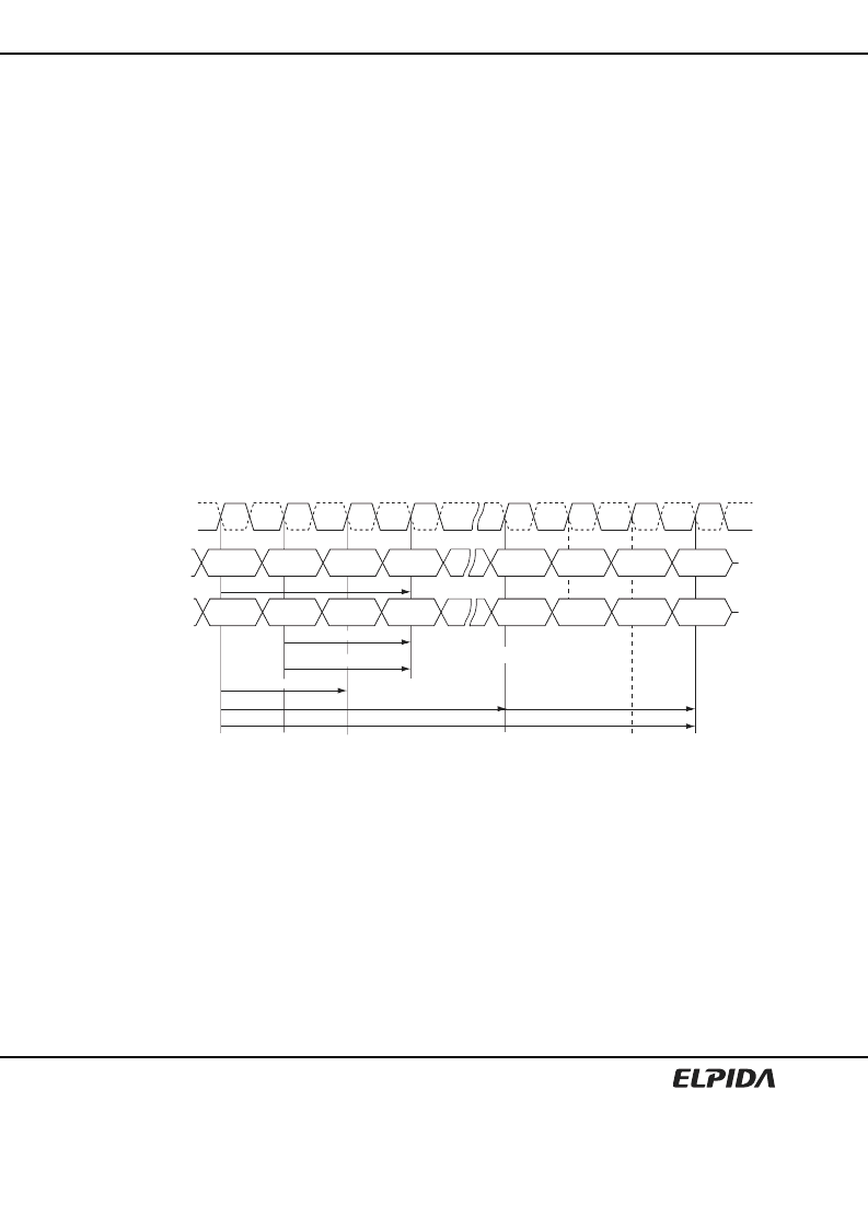
Bank Activate Command [ACT]
The bank activate command is issued by holding /CAS and /WE high with /CS and /RAS low at the rising edge of the
clock. The bank addresses BA0, BA1 and BA2 are used to select the desired bank. The row address A0 through
A13 is used to determine which row to activate in the selected bank. The Bank activate command must be applied
before any read or write operation can be executed. Immediately after the bank active command, the DDR2 SDRAM
can accept a read or write command on the following clock cycle. If a R/W command is issued to a bank that has
not satisfied the tRCD (min.) specification, then additive latency must be programmed into the device to delay when
the R/W command is internally issued to the device. The additive latency value must be chosen to assure tRCD
(min.) is satisfied. Additive latencies of 0, 1, 2, 3 and 4 are supported. Once a bank has been activated it must be
precharged before another bank activate command can be applied to the same bank. The bank active and
precharge times are defined as tRAS and tRP, respectively. The minimum time interval between successive bank
activate commands to the same bank is determined by the /RAS cycle time of the device (tRC), which is equal to
tRAS + tRP. The minimum time interval between successive bank activate commands to the different bank is
determined by (tRRD).
In order to ensure that 8-bank devices do not exceed the instantaneous current supplying capability of 4-bank
devices, a restriction on the number of sequential ACT commands that can be issued must be observed. The rule is
as follows:
Note: 8-bank device sequential bank activation restriction: No more than 4 banks may be activated in a rolling
tFAW window. Converting to clocks is done by dividing tFAW (ns) by tCK (ns) and rounding up to next
integer value. As an example of the rolling window, if (tFAW/tCK) rounds up to 10 clocks, and an activate
command is issued in clock N, no more than three further activate commands may be issued in clock N+1
through N+9.
/CK
CK
Address
Command
T0
T1
T2
T3
Tn
Tn+1
Tn+2
Tn+3
tRCD(min.)
tRAS
tRP
tRC
ROW: 0
ACT
Bank0
Active
Bank Activate Command Cycle (tRCD = 3, AL = 2, tRP = 3, tRRD = 2, tCCD = 2)
Bank1
Active
Bank0
Active
Bank0
Precharge
Bank1
Precharge
Posted
READ
Posted
READ
ACT
PRE
PRE
ACT
COL: 0
ROW: 0
ROW: 1
COL: 1
tCCD
Additive latency (AL)
tRRD
Bank0 Read begins
相關(guān)PDF資料 |
PDF描述 |
|---|---|
| EDE1104ABSE | 1G bits DDR2 SDRAM |
| EDE1104ABSE-4A-E | 1G bits DDR2 SDRAM |
| EDE1104ABSE-5C-E | 1G bits DDR2 SDRAM |
| EDE1104ABSE-6C-E | 1G bits DDR2 SDRAM |
| EDE1104ABSE-6E-E | 1G bits DDR2 SDRAM |
相關(guān)代理商/技術(shù)參數(shù) |
參數(shù)描述 |
|---|---|
| EDE1116ACBG | 制造商:ELPIDA 制造商全稱:Elpida Memory 功能描述:1G bits DDR2 SDRAM |
| EDE1116ACBG-5C-E | 制造商:ELPIDA 制造商全稱:Elpida Memory 功能描述:1G bits DDR2 SDRAM |
| EDE1116ACBG-6E-E | 制造商:ELPIDA 制造商全稱:Elpida Memory 功能描述:1G bits DDR2 SDRAM |
| EDE1116ACBG-8E-E | 制造商:ELPIDA 制造商全稱:Elpida Memory 功能描述:1G bits DDR2 SDRAM |
| EDE1116ACSE | 制造商:ELPIDA 制造商全稱:Elpida Memory 功能描述:1G bits DDR2 SDRAM |
發(fā)布緊急采購(gòu),3分鐘左右您將得到回復(fù)。