- 您現(xiàn)在的位置:買賣IC網(wǎng) > PDF目錄223726 > EDI7P012FLA3602C15 (ELECTRONIC DESIGNS INC) 12M X 8 FLASH 5V PROM CARD, 150 ns, XMA68 PDF資料下載
參數(shù)資料
| 型號: | EDI7P012FLA3602C15 |
| 廠商: | ELECTRONIC DESIGNS INC |
| 元件分類: | PROM |
| 英文描述: | 12M X 8 FLASH 5V PROM CARD, 150 ns, XMA68 |
| 封裝: | PC CARD-68 |
| 文件頁數(shù): | 8/12頁 |
| 文件大小: | 115K |
| 代理商: | EDI7P012FLA3602C15 |
White Electronic Designs
One Research Drive Westborough, MA 01581
http://www.whiteedc.com
PC Card Products
5
July 28, 1999
FLA Series
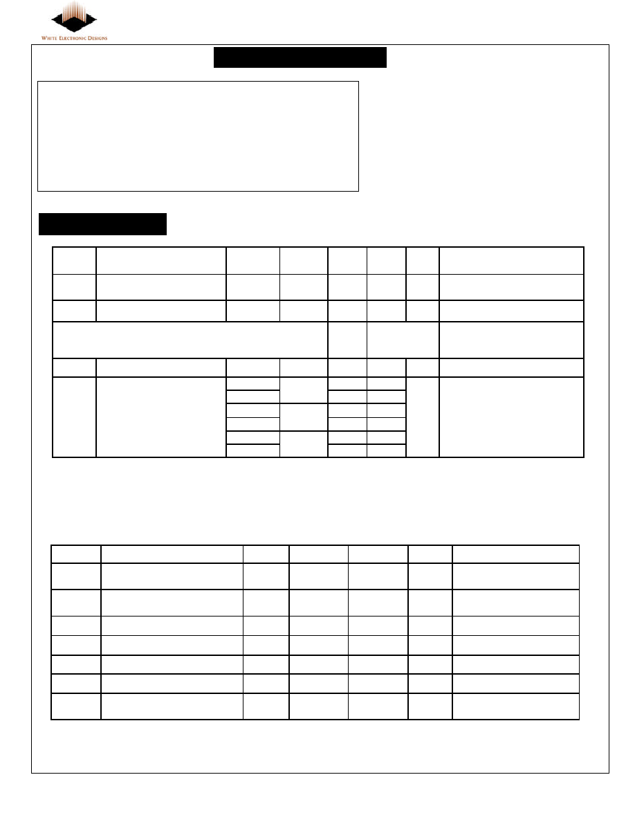
Absolute Maximum Ratings (1)
Operating Temperature TA (ambient)
Commercial
0°C to +60 °C
Industrial
-40°C to +85 °C
Storage Temperature
Commercial
-30°C to +80 °C
Industrial
-40°C to +85 °C
Voltage on any pin relative to VSS
-0.5V to VCC+0.5V
VCC supply Voltage relative to VSS
-0.5V to +7.0V
Notes:
(1) Stress greater than those listed under “Absolute
Maximum ratings” may cause permanent damage
to the device. This is a stress rating only and
functional operation at these or any other conditions
greater than those indicated in the operational
sections of this specification is not implied.
Exposure to absolute maximum rating conditions for
extended periods may affect reliability.
Symbol Parameter
Density
(Mbytes)
Notes
Typ
(3)
Max
Units Test Conditions
ICCR
VCC Read Current
All
35
mA
VCC = VCCmax
tcycle = 150ns,CMOS levels
ICCW
VCC Program Current
All
28F008S5
28F016S5
75
mA
ICCW
VCC Program Current
All
30
mA
IPPW
VPP Program Current
All
28F008SA
Vpp=12V
30
mA
ICCE
VCC Erase Current
All
100
mA
2MB
110
230
20MB
2
28F008SA
900
2MB
60
20MB
2
28F008S5
420
4MB
60
ICCS
(CMOS)
VCC Standby Current
40MB
2
28F016S5
380
A
VCC = VCCmax
Control Signals = VCC
Reset = VSS, CMOS levels
Notes:
1. All currents are RMS values unless otherwise specified. ICCR, ICCW and ICCE are based on Byte wide operations. For 16 bit
operation values are double.
2. Control Signals: CE
1#, CE2#, OE#, WE#, REG#
3. Typical: VCC = 5V, T = +25C
CMOS Test Conditions: VCC = 5V ± 5%, VIL = VSS ± 0.2V, VIH = VCC ± 0.2V
DC Characteristics(1)
Symbol
Parameter
Notes
Min
Max
Units
Test Conditions
ILI
Input Leakage Current
1
±20
A
VCC = VCCMAX
Vin =VCC or VSS
ILO
Output Leakage Current
1
±20
A
VCC = VCCMAX
Vout =VCC or VSS
VIL
Input Low Voltage
1
0
0.8
V
VIH
Input High Voltage
1
0.7VCC
VCC+0.5
V
VOL
Output Low Voltage
1
0.4
V
IOL = 3.2mA
VOH
Output High Voltage
1
VCC-0.4
VCC
V
IOH = -2.0mA
VLKO
VCC Erase/Program
Lock Voltage
1
2.0
V
Notes:
1) Values are the same for byte and word wide modes for all card densities.
2) Exceptions: Leakage currents on CE1#, CE2#, OE#, REG# and WE# will be < 500 A when VIN = GND due to
internal pull-up resistors. Leakage currents on RST will be <150A when VIN=VCC due to internal pull-down resistor
相關(guān)PDF資料 |
PDF描述 |
|---|---|
| EDI7P012FLA6601C15 | 12M X 8 FLASH 5V PROM CARD, 150 ns, XMA68 |
| EDI7P012FLB2602I15 | 12M X 8 FLASH 5V PROM CARD, 150 ns, XMA68 |
| EDI7P032FLB2200C15 | 32M X 8 FLASH 5V PROM CARD, 150 ns, XMA68 |
| EDI7P012FLB2602C15 | 12M X 8 FLASH 5V PROM CARD, 150 ns, XMA68 |
| EDI7P036FLB2201C15 | 36M X 8 FLASH 5V PROM CARD, 150 ns, XMA68 |
相關(guān)代理商/技術(shù)參數(shù) |
參數(shù)描述 |
|---|---|
| EDI7P012FLD2100C15 | 制造商:未知廠家 制造商全稱:未知廠家 功能描述:Peripheral Miscellaneous |
| EDI7P012FLD2100I15 | 制造商:未知廠家 制造商全稱:未知廠家 功能描述:Peripheral Miscellaneous |
| EDI7P012FLD2101C15 | 制造商:未知廠家 制造商全稱:未知廠家 功能描述:Peripheral Miscellaneous |
| EDI7P012FLD2101I15 | 制造商:未知廠家 制造商全稱:未知廠家 功能描述:Peripheral Miscellaneous |
| EDI7P012FLD2102C15 | 制造商:未知廠家 制造商全稱:未知廠家 功能描述:Peripheral Miscellaneous |
發(fā)布緊急采購,3分鐘左右您將得到回復(fù)。