- 您現(xiàn)在的位置:買賣IC網(wǎng) > PDF目錄223726 > EDI7P8FLE232C15 (WHITE ELECTRONIC DESIGNS CORP) 4M X 16 FLASH 5V PROM CARD, 150 ns, XMA68 PDF資料下載
參數(shù)資料
| 型號: | EDI7P8FLE232C15 |
| 廠商: | WHITE ELECTRONIC DESIGNS CORP |
| 元件分類: | PROM |
| 英文描述: | 4M X 16 FLASH 5V PROM CARD, 150 ns, XMA68 |
| 文件頁數(shù): | 9/13頁 |
| 文件大小: | 181K |
| 代理商: | EDI7P8FLE232C15 |
5
White Electronic Designs Corporation (602) 437-1520 www.wedc.com
White Electronic Designs
PCMCIA Flash Memory Card
FLE Series
August 2000
Rev. 4
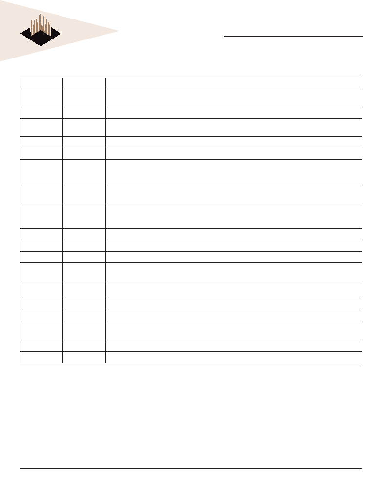
CARD SIGNAL DESCRIPTION
Symbol
Type
Name and Function
A0 - A25
INPUT
ADDRESS INPUTS: A0 through A25 enable direct addressing of up to 64MB of memory on the card. Signal A0 is not
used in word access mode. A25 is the most signicant bit
DQ0 - DQ15
INPUT/OUTPUT
DATA INPUT/OUTPUT: DQ0 THROUGH DQ15 constitute the bi-directional databus. DQ15 is the MSB.
CE1#, CE2#
INPUT
CARD ENABLE 1 AND 2: CE1# enables even byte accesses, CE2# enables odd byte accesses. Multiplexing A0,
CE1# and CE2# allows 8-bit hosts to access all data on DQ0 - DQ7.
OE#
INPUT
OUTPUT ENABLE: Active low signal gating read data from the memory card.
WE#
INPUT
WRITE ENABLE: Active low signal gating write data to the memory card.
RDY/BSY#
OUTPUT
READY/BUSY OUTPUT: Indicates status of internally timed erase or program algorithms. A high output indicates that
the card is ready to accept accesses. A low output indicates that one or more devices in the memory card are busy
with internally timed erase or write activities.
CD1#, CD2#
OUTPUT
CARD DETECT 1 and 2: Provide card insertion detection. These signals are connected to ground internally on the
memory card. The host socket interface circuitry shall supply 10K-ohm or larger pull-up resistors on these signal pins.
WP
OUTPUT
WRITE PROTECT: Write protect reects the status of the Write Protect switch on the memory card. WP set to high
= write protected, providing internal hardware write lockout to the Flash array. If card does not include optional write
protect switch, this signal will be pulled low internally indicating write protect = “off”.
VPP1, VPP2
N.C.
PROGRAM/ERASE POWER SUPPLY: Not connected for 5V only card.
VCC
CARD POWER SUPPLY: 5.0V for all internal circuitry.
GND
GROUND: for all internal circuitry.
REG#
INPUT
ATTRIBUTE MEMORY SELECT: provides access to Flash memory card registers and Card Information Structure in
the Attribute Memory Plane.
RST
INPUT
RESET: Active high signal for placing card in Power-on default state. Reset can be used as a Power-Down signal for
the memory array.
WAIT#
OUTPUT
WAIT: This signal is pulled high internally for compatibility. No wait states are generated.
BVD1, BVD2
OUTPUT
BATTERY VOLTAGE DETECT: These signals are pulled high to maintain SRAM card compatibility.
VS1, VS2
OUTPUT
VOLTAGE SENSE: Noties the host socket of the card’s VCC requirements. VS1 and VS2 are open to indicate a 5V
card has been inserted.
RFU
RESERVED FOR FUTURE USE
N.C.
NO INTERNAL CONNECTION TO CARD: pin may be driven or left oating
相關(guān)PDF資料 |
PDF描述 |
|---|---|
| EDI816256CA25N44B | 256K X 16 STANDARD SRAM, 25 ns, CDSO44 |
| EDI84256CS55TI | 256K X 4 STANDARD SRAM, 55 ns, CDIP28 |
| EDI88257LPA45CC | 256K X 8 STANDARD SRAM, 45 ns, CDIP32 |
| EDI8832P120QB | 32K X 8 STANDARD SRAM, 120 ns, CDIP28 |
| EDI8908LPA70QM | 8K X 9 STANDARD SRAM, 70 ns, CDIP28 |
相關(guān)代理商/技術(shù)參數(shù) |
參數(shù)描述 |
|---|---|
| EDI816256CA | 制造商:WEDC 制造商全稱:White Electronic Designs Corporation 功能描述:256Kx16 MONOLITHIC SRAM, SMD 5962-96795 |
| EDI816256CA/LPA-F44 | 制造商:未知廠家 制造商全稱:未知廠家 功能描述:SRAM |
| EDI816256CA/LPA-N44 | 制造商:未知廠家 制造商全稱:未知廠家 功能描述:SRAM |
| EDI816256CA17F44B | 制造商:Microsemi Corporation 功能描述:256K X 16 SRAM MONOLITHIC, 5V, 17NS, 44 FLATPACK, TINNED LEA - Bulk |
| EDI816256CA17N44B | 制造商:Microsemi Corporation 功能描述:256K X 16 SRAM MONOLITHIC, 5V, 17NS, 44 CSOJ, TINNED LEADS, - Bulk |
發(fā)布緊急采購,3分鐘左右您將得到回復(fù)。