- 您現(xiàn)在的位置:買賣IC網(wǎng) > PDF目錄362620 > EL2250CS-T7 (ELANTEC) 125MHz Single Supply Dual/Quad Op Amps PDF資料下載
參數(shù)資料
| 型號(hào): | EL2250CS-T7 |
| 廠商: | ELANTEC |
| 元件分類: | 音頻/視頻放大 |
| 英文描述: | 125MHz Single Supply Dual/Quad Op Amps |
| 中文描述: | 2 CHANNEL, VIDEO AMPLIFIER, PDSO8 |
| 封裝: | SO-8 |
| 文件頁數(shù): | 11/15頁 |
| 文件大小: | 419K |
| 代理商: | EL2250CS-T7 |
11
FN7061.2
June 7, 2005
The output range of the EL2250/EL2450 is also quite large.
It includes the negative rail, and extends to within 1V of the
top supply rail with a 1k
load. On a +5V supply, the output
is therefore capable of swinging from 0V to +4V. On split
supplies, the output will swing ±4V. If the load resistor is tied
to the negative rail and split supplies are used, the output
range is extended to the negative rail.
Choice Of Feedback Resistor, R
F
The feedback resistor forms a pole with the input
capacitance. As this pole becomes larger, phase margin is
reduced. This increases ringing in the time domain and
peaking in the frequency domain. Therefore, R
F
has some
maximum value which should not be exceeded for optimum
performance. If a large value of R
F
must be used, a small
capacitor in the few picofarad range in parallel with R
F
can
help to reduce this ringing and peaking at the expense of
reducing the bandwidth.
As far as the output stage of the amplifier is concerned,
R
F
+ R
G
appear in parallel with R
L
for gains other than +1.
As this combination gets smaller, the bandwidth falls off.
Consequently, R
F
has a minimum value that should not be
exceeded for optimum performance.
For A
V
= +1, R
F
= 0
is optimum. For A
V
= -1 or +2 (noise
gain of 2), optimum response is obtained with R
F
between
500
and 1k
. For Av = -4 or +5 (noise gain of 5), keep R
F
between 2k
and 10k
.
Video Performance
For good video performance, an amplifier is required to
maintain the same output impedance and the same
frequency response as DC levels are changed at the output.
This can be difficult when driving a standard video load of
150
, because of the change in output current with DC level.
Differential Gain and Differential Phase for the
EL2250/EL2450 are specified with the black level of the
output video signal set to +1.2V. This allows ample room for
the sync pulse even in a gain of +2 configuration. This
results in dG and dP specifications of 0.05% and 0.05° while
driving 150
at a gain of +2. Setting the black level to other
values, although acceptable, will compromise peak
performance. For example, looking at the single supply dG
and dP curves for R
L
=150
, if the output black level clamp is
reduced from 1.2V to 0.6V dG/dP will increase from
0.05%/0.05° to 0.08%/0.25° Note that in a gain of +2
configuration, this is the lowest black level allowed such that
the sync tip doesn’t go below 0V.
If your application requires that the output goes to ground,
then the output stage of the EL2250/EL2450, like all other
single supply op amps, requires an external pull down
resistor tied to ground. As mentioned above, the current
flowing through this resistor becomes the DC bias current for
the output stage NPN transistor. As this current approaches
zero, the NPN turns off, and dG and dP will increase. This
becomes more critical as the load resistor is increased in
value. While driving a light load, such as 1k
, if the input
black level is kept above 1.25V, dG and dP are a respectable
0.03% and 0.03°.
For other biasing conditions see the Differential Gain and
Differential Phase vs. Input Voltage curves.
Output Drive Capability
In spite of their moderately low 5mA of supply current, the
EL2250/EL2450 are capable of providing ±100mA of output
current into a 10
load, or ±60mA into 50
. With this large
output current capability, a 50
load can be driven to ±3V
with V
S
= ±5V, making it an excellent choice for driving
isolation transformers in telecommunications applications.
Driving Cables and Capacitive Loads
When used as a cable driver, double termination is always
recommended for reflection-free performance. For those
applications, the back-termination series resistor will de-
couple the EL2250/EL2450 from the cable and allow
extensive capacitive drive. However, other applications may
have high capacitive loads without a back-termination
resistor. In these applications, a small series resistor (usually
between 5
and 50
) can be placed in series with the
output to eliminate most peaking. The gain resistor (R
G
) can
then be chosen to make up for any gain loss which may be
created by this additional resistor at the output.
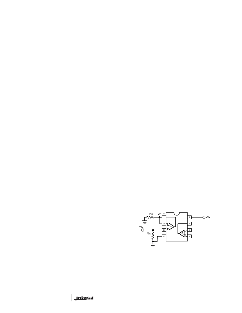
Video Sync Pulse Remover Application
All CMOS Analog to Digital Converters (A/Ds) have a
parasitic latch-up problem when subjected to negative input
voltage levels. Since the sync tip contains no useful video
information and it is a negative going pulse, we can chop it
off.
Figure 1 shows a unity gain connected amplifier A of an
EL2250. Figure 2 shows the complete input video signal
applied at the input, as well as the output signal with the
negative going sync pulse removed.
FIGURE 1.
EL2250, EL2450
相關(guān)PDF資料 |
PDF描述 |
|---|---|
| EL2250CSZ | 125MHz Single Supply Dual/Quad Op Amps |
| EL2250CSZ-T7 | 125MHz Single Supply Dual/Quad Op Amps |
| EL2250CSZ-T13 | 125MHz Single Supply Dual/Quad Op Amps |
| EL2257 | 125MHz Single Supply, Clamping Op Amp |
| EL2257CN | 125MHz Single Supply, Clamping Op Amp |
相關(guān)代理商/技術(shù)參數(shù) |
參數(shù)描述 |
|---|---|
| EL2250CSZ | 功能描述:高速運(yùn)算放大器 EL2250CSZ 100 MHZ DL OP AMP SNGL SUPY RoHS:否 制造商:Texas Instruments 通道數(shù)量:1 電壓增益 dB:116 dB 輸入補(bǔ)償電壓:0.5 mV 轉(zhuǎn)換速度:55 V/us 工作電源電壓:36 V 電源電流:7.5 mA 最大工作溫度:+ 85 C 安裝風(fēng)格:SMD/SMT 封裝 / 箱體:SOIC-8 封裝:Tube |
| EL2250CSZ-T13 | 功能描述:高速運(yùn)算放大器 EL2250CSZ 100 MHZ DL OP AMP SNGL SUPY RoHS:否 制造商:Texas Instruments 通道數(shù)量:1 電壓增益 dB:116 dB 輸入補(bǔ)償電壓:0.5 mV 轉(zhuǎn)換速度:55 V/us 工作電源電壓:36 V 電源電流:7.5 mA 最大工作溫度:+ 85 C 安裝風(fēng)格:SMD/SMT 封裝 / 箱體:SOIC-8 封裝:Tube |
| EL2250CSZ-T7 | 功能描述:高速運(yùn)算放大器 EL2250CSZ 100 MHZ DL OP AMP SNGL SUPY RoHS:否 制造商:Texas Instruments 通道數(shù)量:1 電壓增益 dB:116 dB 輸入補(bǔ)償電壓:0.5 mV 轉(zhuǎn)換速度:55 V/us 工作電源電壓:36 V 電源電流:7.5 mA 最大工作溫度:+ 85 C 安裝風(fēng)格:SMD/SMT 封裝 / 箱體:SOIC-8 封裝:Tube |
| EL2252 | 制造商:INTERSIL 制造商全稱:Intersil Corporation 功能描述:Dual 50MHz Comparator/Pin Receiver |
| EL2252C | 制造商:ELANTEC 制造商全稱:ELANTEC 功能描述:Dual 50 MHz Comparator/Pin Receiver |
發(fā)布緊急采購,3分鐘左右您將得到回復(fù)。