- 您現(xiàn)在的位置:買賣IC網(wǎng) > PDF目錄353102 > EL4450 (Intersil Corporation) Wideband Four-Quadrant Multiplier PDF資料下載
參數(shù)資料
| 型號: | EL4450 |
| 廠商: | Intersil Corporation |
| 英文描述: | Wideband Four-Quadrant Multiplier |
| 中文描述: | 寬帶四象限乘法器 |
| 文件頁數(shù): | 7/14頁 |
| 文件大小: | 266K |
| 代理商: | EL4450 |
2
EL4450C
Wideband Four-Quadrant Multiplier
E
L
4450C
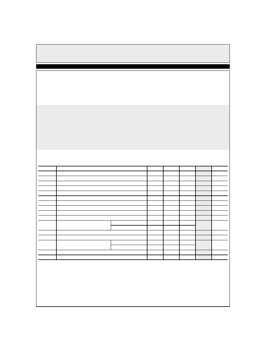
Absolute Maximum Ratings (T
A = 25 °C)
V+
Positive Supply Voltage
16.5V
VS
V+ to V- Supply Voltage
33V
VIN
Voltage at any Input or Feedback
V+ to V-
VIN
Difference between Pairs of Inputs or Feedback
6V
IIN
Current into any Input or Feedback Pin
4 mA
IOUT Output Current
30 mA
PD
Maximum Power Dissipation
See Curves
TA
Operating Temperature Range
-40°C to +85°C
TS
Storage Temperature Range
-60°C to +150°C
Important Note:
All parameters having Min/Max specifications are guaranteed. The Test Level column indicates the specific device testing actually performed during
production and Quality inspection. Elantec performs most electrical tests using modern high-speed automatic test equipment, specifically the LTX77
Series system. Unless otherwise noted, all tests are pulsed tests, therefor TJ = TC = TA.
Test Level
Test Procedure
I
100% production tested and QA sample tested per QA test plan QCX0002.
II
100% production tested at TA = 25°C and QA sample tested at TA = 25°C, TMAX and TMIN per QA test plan QCX0002.
III
QA sample tested per QA test plan QCX0002.
IV
Parameter is guaranteed (but not tested) by Design and Characterization Data.
V
Parameter is typical value at TA = 25°C for information purposes only.
Open-Loop DC Electrical Characteristics
Power Supplies at ±5V, TA = 25°C, VFB = VOUT.
Parameter
Description
Min
Typ
Max
Test Level
Units
VDIFF
Differential Input Voltage—Clipping
1.8
2.0
IV
0.2% nonlinearity
1.0
VV
VCM
Common-Mode Range of VDIFF = 0, VS = ±5V
±2.5
±2.8
IV
VS = ±15V
±12.5
±12.8
IV
VOS
Input Offset Voltage
8
35
ImV
IB
Input Bias Current
9
20
IA
IOS
Input Offset Current between XIN+ and XIN-, YIN+ and YIN-, REF and FB
0.5
4
IA
Gain
Gain Factor of VOUT = Gain × XIN+ × YIN
0.45
0.5
0.55
I
V/V
2
NLx
Nonlinearity of X Input; XIN between -1V and +1V
0.3
0.7
I%
NLy
Nonlinearity of Y Input; YIN between -1V and +1V
0.2
0.35
I%
RIN
Input resistance
XIN+ to XIN-, YIN+ to YIN-,
230
Vk
REF to FB
90
CMRR
Common-Mode Rejection Ratio, XIN and YIN
70
90
IdB
PSRR
Power-Supply Rejection Ratio, FB
60
72
IdB
VO
Output Voltage Swing
(VIN = 0, VREF Varied)
VS = ±5V
±2.5
±2.8
IV
VS = ±15V
±12.5
±12.8
ISC
Output Short-Circuit Current
40
85
ImA
IS
Supply Current, VS = ±15V
15.4
18
ImA
D44450B.fm Page 2 Tuesday, April 21, 1998 9:51 AM
相關(guān)PDF資料 |
PDF描述 |
|---|---|
| EL4450CM | Wideband Four-Quadrant Multiplier |
| EL2310CN | Low Cost, Dual, Triple and Quad Video Op Amps |
| EL2310CS | Low Cost, Dual, Triple and Quad Video Op Amps |
| EL2311CN | Low Cost, Dual, Triple and Quad Video Op Amps |
| EL2311CS | Low Cost, Dual, Triple and Quad Video Op Amps |
相關(guān)代理商/技術(shù)參數(shù) |
參數(shù)描述 |
|---|---|
| EL4450C | 制造商:ELANTEC 制造商全稱:ELANTEC 功能描述:Wideband Four-Quadrant Multiplier |
| EL4450CM | 制造商:INTERSIL 制造商全稱:Intersil Corporation 功能描述:Wideband Four-Quadrant Multiplier |
| EL4450CN | 制造商:Rochester Electronics LLC 功能描述: 制造商:Intersil Corporation 功能描述: |
| EL4450CS | 制造商:ELANTEC 制造商全稱:ELANTEC 功能描述:Wideband Four-Quadrant Multiplier |
| EL4451 | 制造商:ELANTEC 制造商全稱:ELANTEC 功能描述:Wideband Variable-Gain Amplifier, Gain of 2 |
發(fā)布緊急采購,3分鐘左右您將得到回復(fù)。