- 您現(xiàn)在的位置:買賣IC網(wǎng) > PDF目錄362635 > EL5283CY (INTERSIL CORP) Replaced by PTN04050A : PDF資料下載
參數(shù)資料
| 型號: | EL5283CY |
| 廠商: | INTERSIL CORP |
| 元件分類: | 模擬信號調理 |
| 英文描述: | Replaced by PTN04050A : |
| 中文描述: | SPECIALTY ANALOG CIRCUIT, PDSO10 |
| 封裝: | MSOP-10 |
| 文件頁數(shù): | 7/8頁 |
| 文件大小: | 150K |
| 代理商: | EL5283CY |
7
Applications Information
Power Supplies and Circuit Layout
The EL5283 comparator operates with single and dual
supply with 5V to 12V between V
S
+ and V
S
-. The output
side of the comparators is supplied by a single supply from
2.7V to 5V. The rail to rail output swing enables direct
connection of the comparator to both CMOS and TTL logic
circuits. As with many high speed devices, the supplies must
be well bypassed. Elantec recommends a 4.7μF tantalum in
parallel with a 0.1μF ceramic. These should be placed as
close as possible to the supply pins. Keep all leads short to
reduce stray capacitance and lead inductance. This will also
minimize unwanted parasitic feedback around the
comparator. The device should be soldered directly to the
PC board instead of using a socket. Use a PC board with a
good, unbroken low inductance ground plane. Good ground
plane construction techniques enhance stability of the
comparators.
Input Voltage Considerations
The EL5283 input range is specified from 0.1V below V
S
- to
2.25V below V
S
+. The criterion for the input limit is that the
output still responds correctly to a small differential input
signal. The differential input stage is a pair of PNP
transistors, therefore, the input bias current flows out of the
device. When either input signal falls below the negative
input voltage limit, the parasitic PN junction formed by the
substrate and the base of the PNP will turn on, resulting in a
significant increase of input bias current. If one of the inputs
goes above the positive input voltage limit, the output will still
maintain the correct logic level as long as the other input
stays within the input range. However, the propagation delay
will increase. When both inputs are outside the input voltage
range, the output becomes unpredictable. Large differential
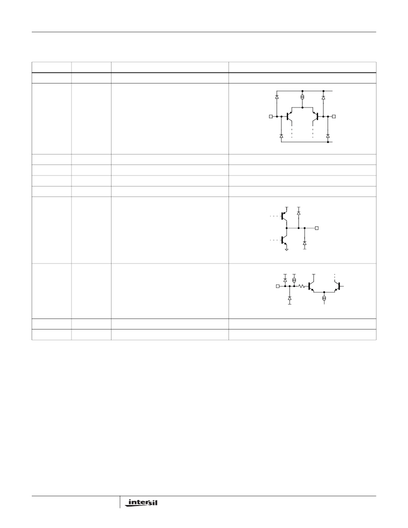
Pin Descriptions
PIN NUMBER
PIN NAME
FUNCTION
EQUIVALENT CIRCUIT
1
VS+
Positive supply voltage
2
VREFH
Upper voltage reference
Circuit 1
3
IN
Input
(Reference Circuit 1)
4
VREFL
Lower voltage reference
(Reference Circuit 1)
5
VS-
Negative supply voltage
6
GDN
Digital ground
7
OUTL
Low output
Circuit 2
8
LATCH
Latch
Circuit 3
9
OUTH
High output
(Reference Circuit 2)
10
VSD
Digital supply voltage
IN
VREF
V
S
+
V
S
-
V
SD
V
S
+
V
S
-
OUT
V
SD
V
S
+
V
S
-
LATCH
V
SD
EL5283
相關PDF資料 |
PDF描述 |
|---|---|
| EL5285CS | Dual 4ns High-Speed Comparator |
| EL5285CS-T13 | Dual 4ns High-Speed Comparator |
| EL5285CS-T7 | Dual 4ns High-Speed Comparator |
| EL5285I | Dual 4ns High-Speed Comparator |
| EL5287 | Replaced by PTN04050A : |
相關代理商/技術參數(shù) |
參數(shù)描述 |
|---|---|
| EL5283CY-T13 | 制造商:INTERSIL 制造商全稱:Intersil Corporation 功能描述:Window 8ns High-Speed Comparator |
| EL5285C | 制造商:ELANTEC 制造商全稱:ELANTEC 功能描述:Dual and Window 4ns High-Speed Comparators |
| EL5285CS | 制造商:INTERSIL 制造商全稱:Intersil Corporation 功能描述:Dual 4ns High-Speed Comparator |
| EL5285CS-T13 | 制造商:INTERSIL 制造商全稱:Intersil Corporation 功能描述:Dual 4ns High-Speed Comparator |
| EL5285CS-T7 | 制造商:INTERSIL 制造商全稱:Intersil Corporation 功能描述:Dual 4ns High-Speed Comparator |
發(fā)布緊急采購,3分鐘左右您將得到回復。