- 您現(xiàn)在的位置:買賣IC網(wǎng) > PDF目錄362635 > EL5285I (Intersil Corporation) Dual 4ns High-Speed Comparator PDF資料下載
參數(shù)資料
| 型號: | EL5285I |
| 廠商: | Intersil Corporation |
| 英文描述: | Dual 4ns High-Speed Comparator |
| 中文描述: | 雙4ns的高速比較器 |
| 文件頁數(shù): | 7/9頁 |
| 文件大小: | 136K |
| 代理商: | EL5285I |
7
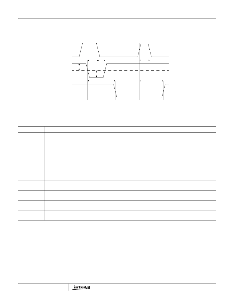
Timing Diagram
Applications Information
Power Supplies and Circuit Layout
The EL5285 comparator operates with single and dual
supply with 5V to 12V between V
S
+ and V
S
-. The output
side of the comparator is supplied by a single supply from
2.7V to 5V. The rail to rail output swing enables direct
connection of the comparator to both CMOS and TTL logic
circuits. As with many high speed devices, the supplies must
be well bypassed. Elantec recommends a 4.7μF tantalum in
parallel with a 0.1μF ceramic. These should be placed as
close as possible to the supply pins. Keep all leads short to
reduce stray capacitance and lead inductance. This will also
minimize unwanted parasitic feedback around the
comparator. The device should be soldered directly to the
PC board instead of using a socket. Use a PC board with a
good, unbroken low inductance ground plane. Good ground
plane construction techniques enhance stability of the
comparators.
Input Voltage Considerations
The EL5285’s input range is specified from 0.1V below V
S
-
to 2.25V below V
S
+. The criterion for the input limit is that
V
IN
V
OD
t
h
t
s
t
pd
-
t
pw
(D)
t
d
+
Latch
Enable
Input
Latch
Compare
Latch
Latch
Compare
Differenti
al Input
Voltage
Comparator
Output
1.4V
V
OS
2.4V
Definition of Terms
TERM
DEFINITION
V
OS
Input Offset Voltage - Voltage applied between the two input terminals to obtain CMOS logic threshold at the output
V
IN
Input Voltage Pulse Amplitude - Usually set to 1V for comparator specifications
V
OD
Input Voltage Overdrive - Usually set to 50mV and in opposite polarity to VIN for comparator specifications
t
pd
+
Input to Output High Delay - The propagation delay measured from the time the input signal crosses the input offset voltage to
the CMOS logic threshold of an output low to high transition
t
pd
-
Input to Output Low Delay - The propagation delay measured from the time the input signal crosses the input offset voltage to
the CMOS logic threshold of an output high to low transition
t
d
+
Latch Disable to Output High Delay - The propagation delay measured from the latch signal crossing the CMOS threshold in a
low to high transition to the point of the output crossing CMOS threshold in a low to high transition
t
d
-
Latch Disable to Output Low Delay - The propagation delay measured from the latch signal crossing the CMOS threshold in a
low to high transition to the point of the output crossing CMOS threshold in a high to low transition
t
s
Minimum Setup Time - The minimum time before the negative transition of the latch signal that an input signal change must be
present in order to be acquired and held at the outputs
t
h
Minimum Hold Time - The minimum time after the negative transition of the latch signal that an input signal must remain
unchanged in order to be acquired and held at the output
t
pw
(D)
Minimum Latch Disable Pulse Width - The minimum time that the latch signal must remain high in order to acquire and hold an
input signal change
EL5285
相關(guān)PDF資料 |
PDF描述 |
|---|---|
| EL5287 | Replaced by PTN04050A : |
| EL5287CY | Replaced by PTN04050A : |
| EL5287CY-T13 | Window 4ns High-Speed Comparator |
| EL5292CS | Replaced by PTN04050C : |
| EL5292CS-T7 | Replaced by PTN04050C : |
相關(guān)代理商/技術(shù)參數(shù) |
參數(shù)描述 |
|---|---|
| EL5287 | 制造商:INTERSIL 制造商全稱:Intersil Corporation 功能描述:Window 4ns High-Speed Comparator |
| EL5287C | 制造商:ELANTEC 制造商全稱:ELANTEC 功能描述:Dual and Window 4ns High-Speed Comparators |
| EL5287CY | 制造商:INTERSIL 制造商全稱:Intersil Corporation 功能描述:Window 4ns High-Speed Comparator |
| EL5287CY-T13 | 制造商:INTERSIL 制造商全稱:Intersil Corporation 功能描述:Window 4ns High-Speed Comparator |
| EL5292 | 制造商:INTERSIL 制造商全稱:Intersil Corporation 功能描述:Dual 600MHz Current Feedback Amplifier with Enable |
發(fā)布緊急采購,3分鐘左右您將得到回復(fù)。