- 您現(xiàn)在的位置:買賣IC網(wǎng) > PDF目錄362651 > EL7563CREZ-T7 (INTERSIL CORP) Monolithic 4 Amp DC:DC Step-Down Regulator PDF資料下載
參數(shù)資料
| 型號: | EL7563CREZ-T7 |
| 廠商: | INTERSIL CORP |
| 元件分類: | 穩(wěn)壓器 |
| 英文描述: | Monolithic 4 Amp DC:DC Step-Down Regulator |
| 中文描述: | 5 A SWITCHING REGULATOR, 1000 kHz SWITCHING FREQ-MAX, PDSO28 |
| 封裝: | ROHS COMPLIANT, MO-153, HTSSOP-28 |
| 文件頁數(shù): | 5/16頁 |
| 文件大小: | 635K |
| 代理商: | EL7563CREZ-T7 |
5
FN7296.2
May 13, 2005
Pin Descriptions
20-PIN SO
(0.300”)
28-PIN
HTSSOP
PIN NAME
PIN FUNCTION
1
1
VREF
Bandgap reference bypass capacitor; typically 0.1μF to SGND
2
2
SGND
Control circuit negative supply or signal ground
3
3
COSC
Oscillator timing capacitor (see performance curves)
4
4
VDD
Control circuit positive supply; normally connected to VIN through an RC filter
5
5
VTJ
Junction temperature monitor; connected with 2.2nF to 3.3nF to SGND
6, 7
6, 7, 8, 9
PGND
Ground return of the regulator; connected to the source of the low-side synchronous NMOS
power FET
8
10, 11
VIN
Power supply input of the regulator; connected to the drain of the high-side NMOS power FET
9
13
STP
Auxiliary supply tracking positive input; tied to regulator output to synchronize start up with a
second supply; leave open for stand alone operation; 2μA internal pull down current
10
14
STN
Auxiliary supply tracking negative input; connect to output of a second supply to synchronize
start up; leave open for stand alone operation; 2μA internal pull up current
11, 12, 13
15, 16
PGND
Ground return of the regulator; connected to the source of the low-side synchronous NMOS
power FET
14, 15
18, 19, 20, 21,
22, 23
LX
Inductor drive pin; high current output whose average voltage equals the regulator output
voltage
16
24
VHI
Positive supply of high-side driver; boot strapped from VDRV to LX with an external 0.22μF
capacitor
17
25
VDRV
Positive supply of low-side driver and input voltage for high side boot strap
18
26
PG
Power good window comparator output; logic 1 when regulator output is within ±10% of target
output voltage
19
27
FB
Voltage feedback input; connected to external resistor divider between VOUT and SGND; a
125nA pull-up current forces VOUT to SGND in the event that FB is floating
20
28
EN
Chip enable, active high; a 2μA internal pull up current enables the device if the pin is left open;
a capacitor can be added at this pin to delay the start of converter
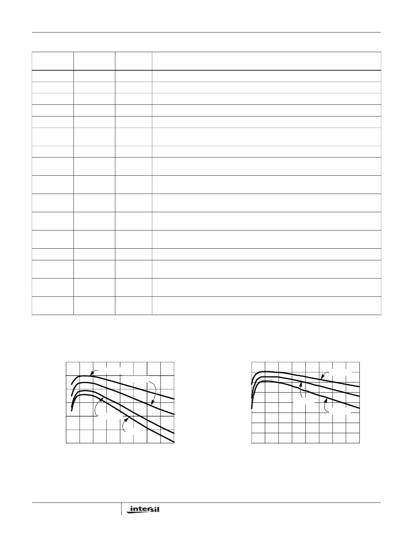
Typical Performance Curves (20 Pin SO Package)
NOTE: The 28-Pin HTSSOP Package Offers Improved Performance
FIGURE 1. EL7563CM EFFICIENCY vs I
O
FIGURE 2. EL7563CRE EFFICIENCY
V
IN
=3.3V
100
95
90
85
80
75
70
0
1
2
2.5
3
3.5
4
LOAD CURRENT I
O
(A)
E
0.5
1.5
V
O
=2.5V
V
O
=1V
V
O
=1.2V
V
O
=1.8V
V
IN
=3.3V
100
95
90
85
80
75
70
65
60
0.1
0.6
1.1
1.6
2.1
2.6
3.1
3.6
4
I
O
(A)
E
V
O
=2.5V
V
O
=1.2V
V
O
=1.8V
EL7563
發(fā)布緊急采購,3分鐘左右您將得到回復。