- 您現(xiàn)在的位置:買賣IC網(wǎng) > PDF目錄362688 > EM78P447SAP (ELAN Microelctronics Corp .) 8-BIT MICRO-CONTROLLER PDF資料下載
參數(shù)資料
| 型號: | EM78P447SAP |
| 廠商: | ELAN Microelctronics Corp . |
| 英文描述: | 8-BIT MICRO-CONTROLLER |
| 中文描述: | 8位微控制器 |
| 文件頁數(shù): | 21/55頁 |
| 文件大小: | 1730K |
| 代理商: | EM78P447SAP |
第1頁第2頁第3頁第4頁第5頁第6頁第7頁第8頁第9頁第10頁第11頁第12頁第13頁第14頁第15頁第16頁第17頁第18頁第19頁第20頁當(dāng)前第21頁第22頁第23頁第24頁第25頁第26頁第27頁第28頁第29頁第30頁第31頁第32頁第33頁第34頁第35頁第36頁第37頁第38頁第39頁第40頁第41頁第42頁第43頁第44頁第45頁第46頁第47頁第48頁第49頁第50頁第51頁第52頁第53頁第54頁第55頁
EM78P447S
OTP ROM
Wake-Up from Pin Change
Bit Name
Power-On
/RESET and WDT
Wake-Up from Pin Change
Bit Name
Power-On
/RESET and WDT
Wake-Up from Pin Change
Bit Name
Power-On
/RESET and WDT
Wake-Up from Pin Change
Bit Name
Power-On
/RESET and WDT
Wake-Up from Pin Change
Bit Name
U
U
U
U
P
U
U
P
/WUE7 /WUE6 /WUE5 /WUE4 /WUE3 /WUE2 /WUE1 /WUE0
1
1
1
1
1
1
1
1
P
P
P
P
X
ODE
WDTE
SLPC
U
0
1
1
U
0
1
1
U
P
1
1
X
X
X
X
U
U
U
U
U
U
U
U
U
U
U
U
-
-
-
-
0
0
0
0
0
0
0
0
P
P
P
P
-
-
-
-
0x0B
0x0E
0x0F
0x08
0x09~
0x3E
IOCB
IOCE
IOCF
R8
1
1
P
1
1
P
X
U
U
U
X
U
U
U
-
0
0
P
-
1
1
P
X
U
U
U
X
U
U
U
-
0
0
P
-
1
1
P
ROC
0
0
P
EXIE
0
0
P
-
0
0
P
-
/WUE
1
1
P
TCIE
0
0
P
-
0
0
P
-
R9~R3E
Power-On
U
U
U
U
U
U
U
U
/RESET and WDT
Wake-Up from Pin Change
P
P
P
P
P
P
P
P
P
P
P
P
P
P
P
P
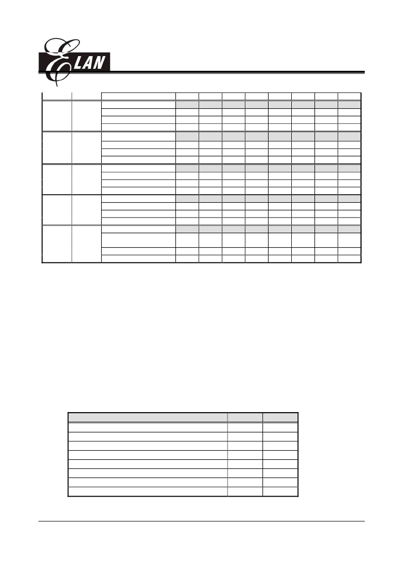
** To execute next instruction after the ”SLPC” bit status of IOCE register being on high-to-low transition.
X: Not used. U: Unknown or don’t care. -: not defined. P: Previous value before reset. t: Check Table 6
2. The Status of RST, T, and P of STATUS Register
A RESET condition is initiated by one of the following events:
1. A power-on condition,
2. A high-low-high pulse on /RESET pin, and
3. Watchdog timer time-out.
The values of T and P (listed in Table 5 below) are used to verify the event that triggered the processor to wake up.
Table 6 shows the events that may affect the status of T and P.
Table 6 The Values of RST, T and P after RESET
Reset Type
T
1
*P
1
*P
0
0
0
*P
P
1
*P
0
*P
*P
0
*P
*P
Power on
/RESET during Operating mode
/RESET wake-up during SLEEP1 mode
/RESET wake-up during SLEEP2 mode
WDT during Operating mode
WDT wake-up during SLEEP1 mode
WDT wake-up during SLEEP2 mode
Wake-Up on pin change during SLEEP2 mode
*P: Previous status before reset
This specification is subject to change without prior notice.
06.25.2003 (V1.1)
21
相關(guān)PDF資料 |
PDF描述 |
|---|---|
| EM78P447SAS | 8-BIT MICRO-CONTROLLER |
| EM78P447SBP | 8-BIT MICRO-CONTROLLER |
| EM78P447SBWM | 8-BIT MICRO-CONTROLLER |
| EM78P447NAM | 8-BIT MICRO-CONTROLLER |
| EM78P447NAP | 8-BIT MICRO-CONTROLLER |
相關(guān)代理商/技術(shù)參數(shù) |
參數(shù)描述 |
|---|---|
| EM7A8620 | 制造商:EMC 制造商全稱:ELAN Microelectronics Corp 功能描述:Voice over IP |
| EM7G | 制造商:GULFSEMI 制造商全稱:Gulf Semiconductor 功能描述:ULTRAFAST EFFICIENT PLASTIC SILICON RECTIFIER VOLTAGE: 1000V CURRENT: 1.0A |
| EM800 | 制造商:EDI 制造商全稱:Electronic devices inc. 功能描述:HIGH VOLTAGE HIGH CURRENT MINIATURE RECTIFIERS |
| EM8000EHP | 制造商:JDSU 制造商全稱:JDS Uniphase Corporation 功能描述:The industrya??s most compact 100 G test solution |
| EM800-DCM | 制造商:MRV 制造商全稱:MRV 功能描述:LambdaDriver Dispersion Compensation Module (EM800/1600-DCM and DCMD) |
發(fā)布緊急采購,3分鐘左右您將得到回復(fù)。