- 您現(xiàn)在的位置:買賣IC網(wǎng) > PDF目錄362739 > EP1K30 (Altera Corporation) ACEX 1K Programmable Logic Family(ACEX 1K 系列可編程邏輯) PDF資料下載
參數(shù)資料
| 型號: | EP1K30 |
| 廠商: | Altera Corporation |
| 英文描述: | ACEX 1K Programmable Logic Family(ACEX 1K 系列可編程邏輯) |
| 中文描述: | ACEX一千可編程邏輯系列(ACEX每1000系列可編程邏輯) |
| 文件頁數(shù): | 3/84頁 |
| 文件大小: | 1366K |
| 代理商: | EP1K30 |
第1頁第2頁當前第3頁第4頁第5頁第6頁第7頁第8頁第9頁第10頁第11頁第12頁第13頁第14頁第15頁第16頁第17頁第18頁第19頁第20頁第21頁第22頁第23頁第24頁第25頁第26頁第27頁第28頁第29頁第30頁第31頁第32頁第33頁第34頁第35頁第36頁第37頁第38頁第39頁第40頁第41頁第42頁第43頁第44頁第45頁第46頁第47頁第48頁第49頁第50頁第51頁第52頁第53頁第54頁第55頁第56頁第57頁第58頁第59頁第60頁第61頁第62頁第63頁第64頁第65頁第66頁第67頁第68頁第69頁第70頁第71頁第72頁第73頁第74頁第75頁第76頁第77頁第78頁第79頁第80頁第81頁第82頁第83頁第84頁
Altera Corporation
3
Preliminary Information
ACEX 1K Programmable Logic Family Data Sheet
D
13
T
I
Software design support and automatic place-and-route provided by
Altera’s MAX+PLUS
II development system for Windows-based
PCs and Sun SPARCstation, HP 9000 Series 700/800, and IBM RISC
System/6000 workstations
Flexible package options are available in 100 to 484 pins, including
the innovative FineLine BGA
TM
packages (see
Tables 2
and
3
)
Additional design entry and simulation support provided by EDIF
2 0 0 and 3 0 0 netlist files, library of parameterized modules (LPM),
DesignWare components, Verilog HDL, VHDL, and other interfaces
to popular EDA tools from manufacturers such as Cadence,
Exemplar Logic, Mentor Graphics, OrCAD, Synopsys, Synplicity,
VeriBest, and Viewlogic
I
I
Notes:
(1)
(2)
Contact Altera Customer Marketing for up-to-date information on package availability.
ACEX 1K device package types include thin quad flat pack (TQFP), plastic quad flat pack (PQFP), and FineLine
BGA packages.
Devices in the same package are pin-compatible, although some devices have more I/O pins than others. When
planning device migration, use the I/O pins that are common to all devices.
Consult Altera Applications for I/O pin count for this package.
This option is supported with a 256-pin FineLine BGA package. By using SameFrame
TM
pin migration, all FineLine
BGA packages are pin-compatible. For example, a board can be designed to support 256-pin and 484-pin FineLine
BGA packages.
(3)
(4)
(5)
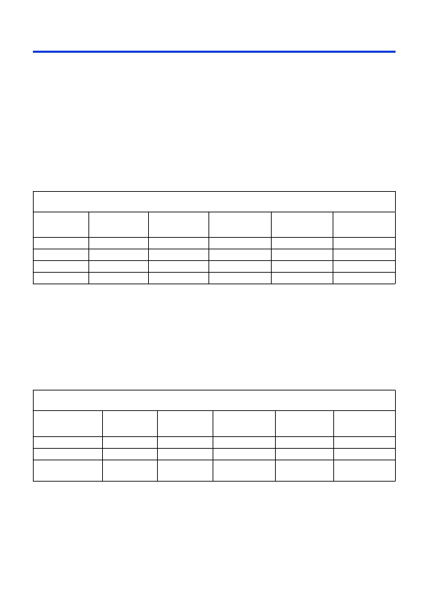
Table 2. ACEX 1K Package Options & I/O Pin Count
Notes (1)
,
(2)
,
(3)
Device
100-Pin TQFP
144-Pin TQFP
208-Pin PQFP
256-Pin
FineLine BGA
484-Pin
FineLine BGA
EP1K10
EP1K30
EP1K50
EP1K100
(4)
102
102
102
130
147
147
147
130
171
186
186
130
171
249
333
(5)
(5)
Table 3. ACEX 1K Package Sizes
Device
100-Pin TQFP
144-Pin TQFP
208-Pin PQFP
256-Pin
FineLine BGA
484-Pin
FineLine BGA
Pitch (mm)
Area (mm
2
)
Length
×
width
(mm
×
mm)
0.50
256
16
×
16
0.50
484
22
×
22
0.50
936
1.0
289
17
×
17
1.0
529
23
×
23
30.6
×
30.6
相關PDF資料 |
PDF描述 |
|---|---|
| EP1K50 | ACEX 1K Programmable Logic Family(ACEX 1K 系列可編程邏輯) |
| EP1K30TI144-2 | Dual LDO with Low Noise, Low IQ, and High PSRR; Temperature Range: -40°C to 85°C; Package: 10-DFN |
| EP1K10 | Programmable Logic Device Family |
| EP1K100 | Programmable Logic Device Family |
| EP1K30 | Programmable Logic Device Family |
相關代理商/技術參數(shù) |
參數(shù)描述 |
|---|---|
| EP1K30FC256-1 | 功能描述:FPGA - 現(xiàn)場可編程門陣列 FPGA - ACEX 1K 216 LABs 171 IOs RoHS:否 制造商:Altera Corporation 系列:Cyclone V E 柵極數(shù)量: 邏輯塊數(shù)量:943 內(nèi)嵌式塊RAM - EBR:1956 kbit 輸入/輸出端數(shù)量:128 最大工作頻率:800 MHz 工作電源電壓:1.1 V 最大工作溫度:+ 70 C 安裝風格:SMD/SMT 封裝 / 箱體:FBGA-256 |
| EP1K30FC256-1N | 功能描述:FPGA - 現(xiàn)場可編程門陣列 FPGA - ACEX 1K 216 LABs 171 IOs RoHS:否 制造商:Altera Corporation 系列:Cyclone V E 柵極數(shù)量: 邏輯塊數(shù)量:943 內(nèi)嵌式塊RAM - EBR:1956 kbit 輸入/輸出端數(shù)量:128 最大工作頻率:800 MHz 工作電源電壓:1.1 V 最大工作溫度:+ 70 C 安裝風格:SMD/SMT 封裝 / 箱體:FBGA-256 |
| EP1K30FC256-2 | 功能描述:FPGA - 現(xiàn)場可編程門陣列 FPGA - ACEX 1K 216 LABs 171 IOs RoHS:否 制造商:Altera Corporation 系列:Cyclone V E 柵極數(shù)量: 邏輯塊數(shù)量:943 內(nèi)嵌式塊RAM - EBR:1956 kbit 輸入/輸出端數(shù)量:128 最大工作頻率:800 MHz 工作電源電壓:1.1 V 最大工作溫度:+ 70 C 安裝風格:SMD/SMT 封裝 / 箱體:FBGA-256 |
| EP1K30FC256-2N | 功能描述:FPGA - 現(xiàn)場可編程門陣列 FPGA - ACEX 1K 216 LABs 171 IOs RoHS:否 制造商:Altera Corporation 系列:Cyclone V E 柵極數(shù)量: 邏輯塊數(shù)量:943 內(nèi)嵌式塊RAM - EBR:1956 kbit 輸入/輸出端數(shù)量:128 最大工作頻率:800 MHz 工作電源電壓:1.1 V 最大工作溫度:+ 70 C 安裝風格:SMD/SMT 封裝 / 箱體:FBGA-256 |
| EP1K30FC256-3 | 功能描述:FPGA - 現(xiàn)場可編程門陣列 FPGA - ACEX 1K 216 LABs 171 IOs RoHS:否 制造商:Altera Corporation 系列:Cyclone V E 柵極數(shù)量: 邏輯塊數(shù)量:943 內(nèi)嵌式塊RAM - EBR:1956 kbit 輸入/輸出端數(shù)量:128 最大工作頻率:800 MHz 工作電源電壓:1.1 V 最大工作溫度:+ 70 C 安裝風格:SMD/SMT 封裝 / 箱體:FBGA-256 |
發(fā)布緊急采購,3分鐘左右您將得到回復。