- 您現(xiàn)在的位置:買賣IC網 > PDF目錄295884 > EP1SGX25CF1020I6ES (ALTERA CORP) FPGA, PBGA1020 PDF資料下載
參數(shù)資料
| 型號: | EP1SGX25CF1020I6ES |
| 廠商: | ALTERA CORP |
| 元件分類: | FPGA |
| 英文描述: | FPGA, PBGA1020 |
| 封裝: | 33 X 33 MM, 1 MM PITCH, FBGA-1020 |
| 文件頁數(shù): | 248/279頁 |
| 文件大小: | 3671K |
| 代理商: | EP1SGX25CF1020I6ES |
第1頁第2頁第3頁第4頁第5頁第6頁第7頁第8頁第9頁第10頁第11頁第12頁第13頁第14頁第15頁第16頁第17頁第18頁第19頁第20頁第21頁第22頁第23頁第24頁第25頁第26頁第27頁第28頁第29頁第30頁第31頁第32頁第33頁第34頁第35頁第36頁第37頁第38頁第39頁第40頁第41頁第42頁第43頁第44頁第45頁第46頁第47頁第48頁第49頁第50頁第51頁第52頁第53頁第54頁第55頁第56頁第57頁第58頁第59頁第60頁第61頁第62頁第63頁第64頁第65頁第66頁第67頁第68頁第69頁第70頁第71頁第72頁第73頁第74頁第75頁第76頁第77頁第78頁第79頁第80頁第81頁第82頁第83頁第84頁第85頁第86頁第87頁第88頁第89頁第90頁第91頁第92頁第93頁第94頁第95頁第96頁第97頁第98頁第99頁第100頁第101頁第102頁第103頁第104頁第105頁第106頁第107頁第108頁第109頁第110頁第111頁第112頁第113頁第114頁第115頁第116頁第117頁第118頁第119頁第120頁第121頁第122頁第123頁第124頁第125頁第126頁第127頁第128頁第129頁第130頁第131頁第132頁第133頁第134頁第135頁第136頁第137頁第138頁第139頁第140頁第141頁第142頁第143頁第144頁第145頁第146頁第147頁第148頁第149頁第150頁第151頁第152頁第153頁第154頁第155頁第156頁第157頁第158頁第159頁第160頁第161頁第162頁第163頁第164頁第165頁第166頁第167頁第168頁第169頁第170頁第171頁第172頁第173頁第174頁第175頁第176頁第177頁第178頁第179頁第180頁第181頁第182頁第183頁第184頁第185頁第186頁第187頁第188頁第189頁第190頁第191頁第192頁第193頁第194頁第195頁第196頁第197頁第198頁第199頁第200頁第201頁第202頁第203頁第204頁第205頁第206頁第207頁第208頁第209頁第210頁第211頁第212頁第213頁第214頁第215頁第216頁第217頁第218頁第219頁第220頁第221頁第222頁第223頁第224頁第225頁第226頁第227頁第228頁第229頁第230頁第231頁第232頁第233頁第234頁第235頁第236頁第237頁第238頁第239頁第240頁第241頁第242頁第243頁第244頁第245頁第246頁第247頁當前第248頁第249頁第250頁第251頁第252頁第253頁第254頁第255頁第256頁第257頁第258頁第259頁第260頁第261頁第262頁第263頁第264頁第265頁第266頁第267頁第268頁第269頁第270頁第271頁第272頁第273頁第274頁第275頁第276頁第277頁第278頁第279頁
4–4
Altera Corporation
Stratix GX Device Handbook, Volume 1
February 2005
Logic Elements
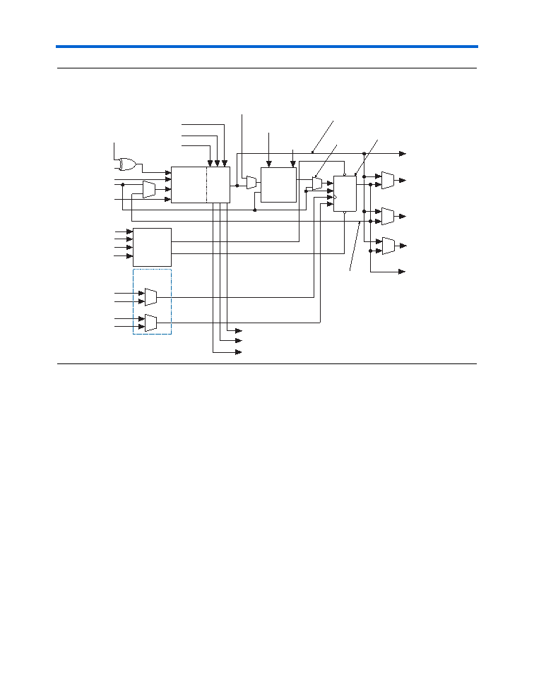
Figure 4–4. Stratix GX LE
Each LE’s programmable register can be configured for D, T, JK, or SR
operation. Each register has data, true asynchronous load data, clock,
clock enable, clear, and asynchronous load/preset inputs. Global signals,
general-purpose I/O pins, or any internal logic can drive the register’s
clock and clear control signals. Either general-purpose I/O pins or
internal logic can drive the clock enable, preset, asynchronous load, and
asynchronous data. The asynchronous load data input comes from the
data3 input of the LE. For combinatorial functions, the register is
bypassed and the output of the LUT drives directly to the outputs of the
LE.
Each LE has three outputs that drive the local, row, and column routing
resources. The LUT or register output can drive these three outputs
independently. Two LE outputs drive column or row and direct link
routing connections and one drives local interconnect resources. This
allows the LUT to drive one output while the register drives another
output. This feature, called register packing, improves device utilization
because the device can use the register and the LUT for unrelated
functions. Another special packing mode allows the register output to
feed back into the LUT of the same LE so that the register is packed with
labclk1
labclk2
labclr2
labpre/aload
Carry-In1
Carry-In0
LAB Carry-In
Clock &
Clock Enable
Select
LAB Carry-Out
Carry-Out1
Carry-Out0
Look-Up
Table
(LUT)
Carry
Chain
Row, column,
and direct link
routing
Row, column,
and direct link
routing
Programmable
Register
PRN/ALD
CLRN
D
Q
ENA
Register Bypass
Packed
Register Select
Chip-Wide
Reset
labclkena1
labclkena2
Synchronous
Load and
Clear Logic
LAB-wide
Synchronous
Load
LAB-wide
Synchronous
Clear
Asynchronous
Clear/Preset/
Load Logic
data1
data2
data3
data4
LUT chain
routing to next LE
labclr1
Local Routing
Register chain
output
ADATA
addnsub
Register
Feedback
Register chain
routing from
previous LE
相關PDF資料 |
PDF描述 |
|---|---|
| EP1SGX25CF1020I6N | FPGA, PBGA1020 |
| EP1SGX25CF1020I7ES | FPGA, PBGA1020 |
| EP1SGX25CF1020I7N | FPGA, PBGA1020 |
| EP1SGX25CF672C5ES | FPGA, PBGA672 |
| EP1SGX25CF672C6ES | FPGA, PBGA672 |
相關代理商/技術參數(shù) |
參數(shù)描述 |
|---|---|
| EP1SGX25CF672C5 | 功能描述:FPGA - 現(xiàn)場可編程門陣列 FPGA - Stratix I GX 2566 LABs 455 IOs RoHS:否 制造商:Altera Corporation 系列:Cyclone V E 柵極數(shù)量: 邏輯塊數(shù)量:943 內嵌式塊RAM - EBR:1956 kbit 輸入/輸出端數(shù)量:128 最大工作頻率:800 MHz 工作電源電壓:1.1 V 最大工作溫度:+ 70 C 安裝風格:SMD/SMT 封裝 / 箱體:FBGA-256 |
| EP1SGX25CF672C5N | 功能描述:FPGA - 現(xiàn)場可編程門陣列 FPGA - Stratix I GX 2566 LABs 455 IOs RoHS:否 制造商:Altera Corporation 系列:Cyclone V E 柵極數(shù)量: 邏輯塊數(shù)量:943 內嵌式塊RAM - EBR:1956 kbit 輸入/輸出端數(shù)量:128 最大工作頻率:800 MHz 工作電源電壓:1.1 V 最大工作溫度:+ 70 C 安裝風格:SMD/SMT 封裝 / 箱體:FBGA-256 |
| EP1SGX25CF672C6 | 功能描述:FPGA - 現(xiàn)場可編程門陣列 FPGA - Stratix I GX 2566 LABs 455 IOs RoHS:否 制造商:Altera Corporation 系列:Cyclone V E 柵極數(shù)量: 邏輯塊數(shù)量:943 內嵌式塊RAM - EBR:1956 kbit 輸入/輸出端數(shù)量:128 最大工作頻率:800 MHz 工作電源電壓:1.1 V 最大工作溫度:+ 70 C 安裝風格:SMD/SMT 封裝 / 箱體:FBGA-256 |
| EP1SGX25CF672C6N | 功能描述:FPGA - 現(xiàn)場可編程門陣列 FPGA - Stratix I GX 2566 LABs 455 IOs RoHS:否 制造商:Altera Corporation 系列:Cyclone V E 柵極數(shù)量: 邏輯塊數(shù)量:943 內嵌式塊RAM - EBR:1956 kbit 輸入/輸出端數(shù)量:128 最大工作頻率:800 MHz 工作電源電壓:1.1 V 最大工作溫度:+ 70 C 安裝風格:SMD/SMT 封裝 / 箱體:FBGA-256 |
| EP1SGX25CF672C7 | 功能描述:FPGA - 現(xiàn)場可編程門陣列 FPGA - Stratix I GX 2566 LABs 455 IOs RoHS:否 制造商:Altera Corporation 系列:Cyclone V E 柵極數(shù)量: 邏輯塊數(shù)量:943 內嵌式塊RAM - EBR:1956 kbit 輸入/輸出端數(shù)量:128 最大工作頻率:800 MHz 工作電源電壓:1.1 V 最大工作溫度:+ 70 C 安裝風格:SMD/SMT 封裝 / 箱體:FBGA-256 |
發(fā)布緊急采購,3分鐘左右您將得到回復。