- 您現(xiàn)在的位置:買賣IC網(wǎng) > PDF目錄295885 > EP1SGX25CF672I7ES (ALTERA CORP) FPGA, PBGA672 PDF資料下載
參數(shù)資料
| 型號: | EP1SGX25CF672I7ES |
| 廠商: | ALTERA CORP |
| 元件分類: | FPGA |
| 英文描述: | FPGA, PBGA672 |
| 封裝: | 27 X 27 MM, 1 MM PITCH, FBGA-672 |
| 文件頁數(shù): | 241/279頁 |
| 文件大小: | 3671K |
| 代理商: | EP1SGX25CF672I7ES |
第1頁第2頁第3頁第4頁第5頁第6頁第7頁第8頁第9頁第10頁第11頁第12頁第13頁第14頁第15頁第16頁第17頁第18頁第19頁第20頁第21頁第22頁第23頁第24頁第25頁第26頁第27頁第28頁第29頁第30頁第31頁第32頁第33頁第34頁第35頁第36頁第37頁第38頁第39頁第40頁第41頁第42頁第43頁第44頁第45頁第46頁第47頁第48頁第49頁第50頁第51頁第52頁第53頁第54頁第55頁第56頁第57頁第58頁第59頁第60頁第61頁第62頁第63頁第64頁第65頁第66頁第67頁第68頁第69頁第70頁第71頁第72頁第73頁第74頁第75頁第76頁第77頁第78頁第79頁第80頁第81頁第82頁第83頁第84頁第85頁第86頁第87頁第88頁第89頁第90頁第91頁第92頁第93頁第94頁第95頁第96頁第97頁第98頁第99頁第100頁第101頁第102頁第103頁第104頁第105頁第106頁第107頁第108頁第109頁第110頁第111頁第112頁第113頁第114頁第115頁第116頁第117頁第118頁第119頁第120頁第121頁第122頁第123頁第124頁第125頁第126頁第127頁第128頁第129頁第130頁第131頁第132頁第133頁第134頁第135頁第136頁第137頁第138頁第139頁第140頁第141頁第142頁第143頁第144頁第145頁第146頁第147頁第148頁第149頁第150頁第151頁第152頁第153頁第154頁第155頁第156頁第157頁第158頁第159頁第160頁第161頁第162頁第163頁第164頁第165頁第166頁第167頁第168頁第169頁第170頁第171頁第172頁第173頁第174頁第175頁第176頁第177頁第178頁第179頁第180頁第181頁第182頁第183頁第184頁第185頁第186頁第187頁第188頁第189頁第190頁第191頁第192頁第193頁第194頁第195頁第196頁第197頁第198頁第199頁第200頁第201頁第202頁第203頁第204頁第205頁第206頁第207頁第208頁第209頁第210頁第211頁第212頁第213頁第214頁第215頁第216頁第217頁第218頁第219頁第220頁第221頁第222頁第223頁第224頁第225頁第226頁第227頁第228頁第229頁第230頁第231頁第232頁第233頁第234頁第235頁第236頁第237頁第238頁第239頁第240頁當(dāng)前第241頁第242頁第243頁第244頁第245頁第246頁第247頁第248頁第249頁第250頁第251頁第252頁第253頁第254頁第255頁第256頁第257頁第258頁第259頁第260頁第261頁第262頁第263頁第264頁第265頁第266頁第267頁第268頁第269頁第270頁第271頁第272頁第273頁第274頁第275頁第276頁第277頁第278頁第279頁
3–14
Altera Corporation
Stratix GX Device Handbook, Volume 1
August 2005
Introduction
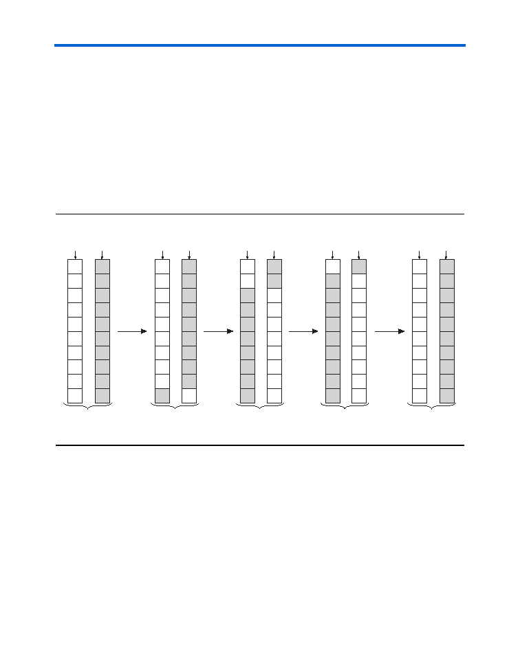
The DPA data-realignment circuitry allows further realignment beyond
what the J multiplication factor allows. You can set the J multiplication
factor to be 8 or 10. However, because data must be continuously clocked
in on each low-speed clock cycle, the upcoming bit to be realigned and
previous n 1 bits of data are selected each time the data realignment
logic’s counter passes n 1. At this point the data is selected entirely from
bit-slip register 3 (see Figure 3–11) as the counter is reset to 0. The logic
array receives a new valid byte of data on the next divided low speed
clock cycle. Figure 3–11 shows the data realignment logic output selection
from data in the data realignment register 2 and data realignment register
3 based on its current counter value upon continuous request of data
slipping from the logic array.
Figure 3–11. DPA Data Realigner
Use the
rx_channel_data_align signal within the device to activate
the data realigner. You can use internal logic or an external pin to control
the
rx_channel_data_align signal. To ensure the rising edge of the
rx_channel_data_align signal is latched into the control logic, the
rx_channel_data_align signal should stay high for at least two low-
frequency clock cycles.
D19
D18
D17
D16
D15
D14
D13
D12
D11
D10
D9
D8
D7
D6
D5
D4
D3
D2
D1
D0
One bit
slipped
Zero bits slipped.
Counter = 0
D10 is the upcoming
bit to be slipped.
Bit Slip
Register 2
Bit Slip
Register 3
D29
D28
D27
D26
D25
D24
D23
D22
D21
D20
D19
D18
D17
D16
D15
D14
D13
D12
D11
D10
Seven more
bits slipped
One bit slipped.
Counter = 1
D21 is the upcoming
bit to be slipped.
Bit Slip
Register 2
Bit Slip
Register 3
D99
D98
D97
D96
D95
D94
D93
D92
D91
D90
D89
D18
D87
D86
D85
D84
D83
D82
D81
D80
One more
bit slipped
One more
bit slipped
Eight bits slipped.
Counter = 8
D98 is the upcoming
bit to be slipped.
Bit Slip
Register 2
Bit Slip
Register 3
D119
D118
D117
D116
D115
D114
D113
D112
D111
D110
Nine bits slipped.
Counter = 9
D119 is the upcoming
bit to be slipped.
Bit Slip
Register 2
Bit Slip
Register 3
D119
D118
D117
D116
D115
D114
D113
D112
D111
D110
D109
D108
D107
D106
D125
D124
D123
D102
D101
D100
10 bits slipped.
Counter = 0
Real data will resume
on the next byte.
Bit Slip
Register 2
Bit Slip
Register 3
D99
D98
D97
D96
D95
D94
D93
D92
D91
D90
相關(guān)PDF資料 |
PDF描述 |
|---|---|
| EP1SGX25CF672I7N | FPGA, PBGA672 |
| EP1SGX25DF1020C5ES | FPGA, PBGA1020 |
| EP1SGX25DF1020C6ES | FPGA, PBGA1020 |
| EP1SGX25DF1020C7ES | FPGA, PBGA1020 |
| EP1SGX25DF1020I5ES | FPGA, PBGA1020 |
相關(guān)代理商/技術(shù)參數(shù) |
參數(shù)描述 |
|---|---|
| EP1SGX25D | 制造商:ALTERA 制造商全稱:Altera Corporation 功能描述:StratixGX FPGA Family |
| EP1SGX25DF1020C5 | 功能描述:FPGA - 現(xiàn)場可編程門陣列 FPGA - Stratix I GX 2566 LABs 607 IOs RoHS:否 制造商:Altera Corporation 系列:Cyclone V E 柵極數(shù)量: 邏輯塊數(shù)量:943 內(nèi)嵌式塊RAM - EBR:1956 kbit 輸入/輸出端數(shù)量:128 最大工作頻率:800 MHz 工作電源電壓:1.1 V 最大工作溫度:+ 70 C 安裝風(fēng)格:SMD/SMT 封裝 / 箱體:FBGA-256 |
| EP1SGX25DF1020C5N | 功能描述:FPGA - 現(xiàn)場可編程門陣列 FPGA - Stratix I GX 2566 LABs 607 IOs RoHS:否 制造商:Altera Corporation 系列:Cyclone V E 柵極數(shù)量: 邏輯塊數(shù)量:943 內(nèi)嵌式塊RAM - EBR:1956 kbit 輸入/輸出端數(shù)量:128 最大工作頻率:800 MHz 工作電源電壓:1.1 V 最大工作溫度:+ 70 C 安裝風(fēng)格:SMD/SMT 封裝 / 箱體:FBGA-256 |
| EP1SGX25DF1020C6 | 功能描述:FPGA - 現(xiàn)場可編程門陣列 FPGA - Stratix I GX 2566 LABs 607 IOs RoHS:否 制造商:Altera Corporation 系列:Cyclone V E 柵極數(shù)量: 邏輯塊數(shù)量:943 內(nèi)嵌式塊RAM - EBR:1956 kbit 輸入/輸出端數(shù)量:128 最大工作頻率:800 MHz 工作電源電壓:1.1 V 最大工作溫度:+ 70 C 安裝風(fēng)格:SMD/SMT 封裝 / 箱體:FBGA-256 |
| EP1SGX25DF1020C6N | 功能描述:FPGA - 現(xiàn)場可編程門陣列 FPGA - Stratix I GX 2566 LABs 607 IOs RoHS:否 制造商:Altera Corporation 系列:Cyclone V E 柵極數(shù)量: 邏輯塊數(shù)量:943 內(nèi)嵌式塊RAM - EBR:1956 kbit 輸入/輸出端數(shù)量:128 最大工作頻率:800 MHz 工作電源電壓:1.1 V 最大工作溫度:+ 70 C 安裝風(fēng)格:SMD/SMT 封裝 / 箱體:FBGA-256 |
發(fā)布緊急采購,3分鐘左右您將得到回復(fù)。