- 您現(xiàn)在的位置:買賣IC網(wǎng) > PDF目錄375714 > FA3641 (FUJI ELECTRIC HOLDINGS CO., LTD.) PWM control IC with light load power saving function For Switching Power Supply Control PDF資料下載
參數(shù)資料
| 型號: | FA3641 |
| 廠商: | FUJI ELECTRIC HOLDINGS CO., LTD. |
| 元件分類: | 基準電壓源/電流源 |
| 英文描述: | PWM control IC with light load power saving function For Switching Power Supply Control |
| 中文描述: | 輕負載的PWM與節(jié)水開關電源控制功能電源控制IC |
| 文件頁數(shù): | 17/21頁 |
| 文件大?。?/td> | 406K |
| 代理商: | FA3641 |

FA3641P(N), FA3647P(N)
74
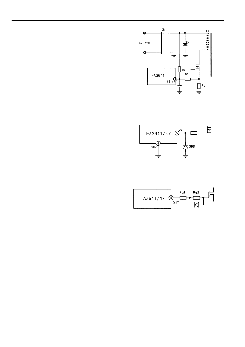
13. Correcting overload detection current (FA3641 only)
If the power supply output is overloaded, the IC overcurrent
limiting function restricts the output power and the overload
shutdown function stops the IC. The output current when an
overload occurs varies depending on the input voltage; the
higher the input voltage, the more the overload detection current
may increase.
If any problems occur as a result of the appearance of this
symptom, connect resistor R8 between current detection
resistor Rs and the IS (+) pin and add resistor R7 for correction
as shown in Figure 32. The standard resistance of R8 is several
hundred ohms, and that of R7 is from several hundred kilohms
to several megohms.
Note that the above correction slightly lowers the output current
when overload even where the input voltage is low. This
correction is available only for the FA3641 that uses positive
polarity for overcurrent detection.
14. Preventing malfunction caused by noise
The IS pin for overcurrent limiting function detects the MOSFET
current converted to the voltage. The parasitic capacitor and
inductor of the MOSFET, transformer, wiring, etc. cause a noise
in switching operation. If this switching noise causes a
malfunction of overcurrent limitimg function, insert the RC filter
into IS pin as shown in Figure 14.
Also, connect a noise prevention capacitor (0.1
μ
F or more) to
the REF pin that outputs the reference voltage for each
component.
15. Preventing malfunction caused by negative voltage
applied to a pin
When large negative voltage is applied to each IC pin, a
parasitic element in the IC may operate and cause malfunction.
Be careful not to allow the voltage applied to each pin to drop
below
–
0.3V.
Especially for the OUT pin, voltage oscillation caused after the
MOSFET turns off may be applied to the OUT pin via the
parasitic capacitance of the MOSFET, causing the negative
voltage to be applied to the OUT pin. If the voltage falls below
–
0.3V, add a Schottky diode between the OUT pin and the
ground. The forward voltage of the Schottky diode can suppress
the voltage applied to the OUT pin.
Use the low forward voltage of the Schottky diode. Similarly, be
careful not to cause the voltages at other pins to fall below
–
0.3V.
16. Gate circuit configuration
To adjust switching speeds or prevent oscillation at gate
terminals, resistors are normally inserted between the power
MOSFET gate terminal to be driven and the OUT pin of the IC.
You may prefer to decide on the drive current independently, to
turn the MOSFET on and off. If so, connect the MOSFET gate
terminal to the OUT pin of the IC as shown in Figure 34.
In the circuit shown in Figure 34, Rg1 and Rg2 restrict the
current when the MOSFET is turned on, and only Rg1 restricts
the current when it is turned off.
Fig. 33 Protection of OUT pin against the negative voltage
Fig. 32 Correcting overload detecting current circuit
Fig. 34 Gate circuit
相關PDF資料 |
PDF描述 |
|---|---|
| FA3641N | PWM control IC with light load power saving function For Switching Power Supply Control |
| FA3641P | PWM control IC with light load power saving function For Switching Power Supply Control |
| FA3647 | PWM control IC with light load power saving function For Switching Power Supply Control |
| FA3647N | PWM control IC with light load power saving function For Switching Power Supply Control |
| FA3647P | PWM control IC with light load power saving function For Switching Power Supply Control |
相關代理商/技術參數(shù) |
參數(shù)描述 |
|---|---|
| FA3641N | 制造商:Panasonic Industrial Company 功能描述:IC |
| FA3641N-H1 | 制造商:Fuji Electric 功能描述: |
| FA3641P | 制造商:FUJI 制造商全稱:Fuji Electric 功能描述:PUJI Power Supply Controllc |
| FA3641P_00 | 制造商:FUJI 制造商全稱:Fuji Electric 功能描述:PUJI Power Supply Controllc |
| FA3641P-D1 | 制造商:Fuji Electric 功能描述: |
發(fā)布緊急采購,3分鐘左右您將得到回復。