- 您現(xiàn)在的位置:買賣IC網(wǎng) > PDF目錄375718 > FAN1587A (Fairchild Semiconductor Corporation) 3A Adjustable/Fixed Low Dropout Linear Regulator PDF資料下載
參數(shù)資料
| 型號: | FAN1587A |
| 廠商: | Fairchild Semiconductor Corporation |
| 英文描述: | 3A Adjustable/Fixed Low Dropout Linear Regulator |
| 中文描述: | 第3A可調(diào)/固定低壓差線性穩(wěn)壓器 |
| 文件頁數(shù): | 8/14頁 |
| 文件大小: | 70K |
| 代理商: | FAN1587A |

FAN1587A
PRODUCT SPECIFICATION
8
REV. 1.0.5 11/10/03
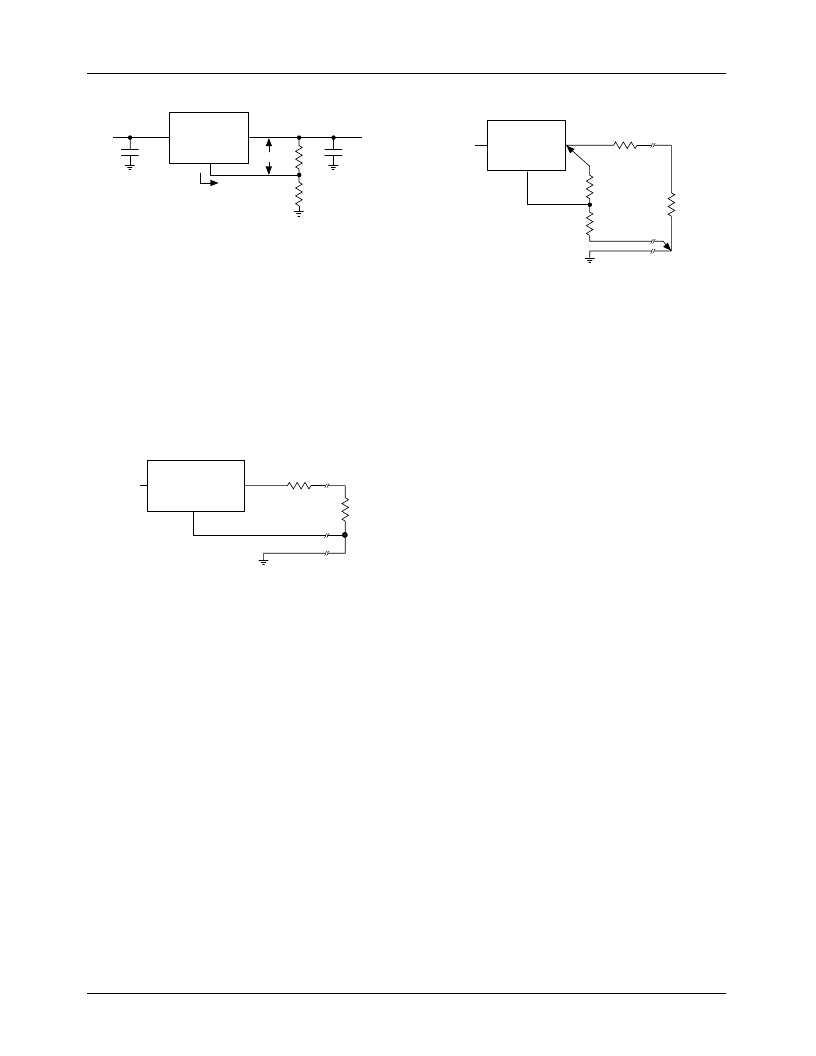
Figure 12. Basic Regulator Circuit
Load Regulation
It is not possible to provide true remote load sensing because
the FAN1587A series are three-terminal devices. Load regu-
lation is limited by the resistance of the wire connecting the
regulators to the load. Load regulation per the data sheet
specification is measured at the bottom of the package.
For fixed voltage devices, negative side sensing is a true
Kelvin connection with the ground pin of the device returned
to the negative side of the load. This is illustrated in
Figure 13.
Figure 13. Connection for Best Load Regulation
For adjustable voltage devices, negative side sensing is a true
Kelvin connection with the bottom of the output divider
returned to the negative side of the load. The best load regu-
lation is obtained when the top of resistor divider R1 con-
nects directly to the regulator output and not to the load.
Figure 14 illustrates this point.
If R1 connects to the load, then the effective resistance
between the regulator and the load would be:
R
P
×
(1 + R2/R1), R
P
= Parasitic Line Resistance
The connection shown in Figure 14 does not multiply R
P
by
the divider ratio. As an example, R
P
is about four milliohms
per foot with 16-gauge wire. This translates to 4mV per foot
at 1A load current. At higher load currents, this drop repre-
sents a significant percentage of the overall regulation. It is
important to keep the positive lead between the regulator and
the load as short as possible and to use large wire or PC
board traces.
Figure 14. Connection for Best Load Regulation
Thermal Considerations
The FAN1587A series protect themselves under overload
conditions with internal power and thermal limiting circuitry.
However, for normal continuous load conditions, do not
exceed maximum junction temperature ratings. It is impor-
tant to consider all sources of thermal resistance from junc-
tion-to-ambient. These sources include the junction-to-case
resistance, the case-to-heat sink interface resistance, and the
heat sink resistance. Thermal resistance specifications have
been developed to more accurately reflect device tempera-
ture and ensure safe operating temperatures.
For example, look at using an FAN1587AT to generate 3A
@ 1.5V
±
2% from a 3.3V source (3.2V to 3.6V).
Assumptions:
V
IN
= 3.6V worst case
V
OUT
= 1.46V worst case
I
OUT
= 3A continuous
T
A
= 70
°
C
θ
Case-to-Ambient
= 3
°
C/W (assuming both a heatsink and
a thermally conductive material)
The power dissipation in this application is:
P
D
= (V
IN
– V
OUT
) * (I
OUT
) = (3.6 – 1.46) * (3) = 6.42W
From the specification table:
T
J
= T
A
+ (P
D
) * (
θ
Case-to-Ambient
+
θ
JC
)
= 70 + (6.42) * (3 + 3) = 109
°
C
The junction temperature is below the maximum rating.
FAN1587A
ADJ
I
ADJ
35
μ
A
R2
R1
C2
22
μ
F
V
OUT
V
REF
+
C1
22
μ
F
+
65-1587-14
IN
V
OUT
= V
REF
(1 + R2/R1) + I
ADJ
(R2)
OUT
V
IN
FAN1587A-1.5, -3.3
IN
GND
R
L
65-1587-17
R
P
PARASITIC
LINE RESISTANCE
OUT
V
IN
FAN1587A
ADJ
R2*
CONNECT R1 TO CASE
CONNECT R2 TO LOAD
*
R1*
R
L
65-1587-15
R
P
PARASITIC
LINE RESISTANCE
IN
OUT
V
IN
相關(guān)PDF資料 |
PDF描述 |
|---|---|
| FAN1587ADX | 3A Adjustable/Fixed Low Dropout Linear Regulator |
| FAN1587AMX | PCB PIN STRIP 8113 S /16 W OB SW RoHS Compliant: Yes |
| FAN1587AMC15X | 3A Adjustable/Fixed Low Dropout Linear Regulator |
| FAN1587AMC33X | 3A Adjustable/Fixed Low Dropout Linear Regulator |
| FAN1587AMCX | 3A Adjustable/Fixed Low Dropout Linear Regulator |
相關(guān)代理商/技術(shù)參數(shù) |
參數(shù)描述 |
|---|---|
| FAN1587AD | 制造商:未知廠家 制造商全稱:未知廠家 功能描述:Positive Adjustable Voltage Regulator |
| FAN1587AD-1.5 | 制造商:未知廠家 制造商全稱:未知廠家 功能描述:Positive Fixed Voltage Regulator |
| FAN1587AD15X | 功能描述:低壓差穩(wěn)壓器 - LDO 3a adj/Fixed LDO RoHS:否 制造商:Texas Instruments 最大輸入電壓:36 V 輸出電壓:1.4 V to 20.5 V 回動電壓(最大值):307 mV 輸出電流:1 A 負載調(diào)節(jié):0.3 % 輸出端數(shù)量: 輸出類型:Fixed 最大工作溫度:+ 125 C 安裝風(fēng)格:SMD/SMT 封裝 / 箱體:VQFN-20 |
| FAN1587AD-3.3 | 制造商:未知廠家 制造商全稱:未知廠家 功能描述:Positive Fixed Voltage Regulator |
| FAN1587AD33X | 功能描述:低壓差穩(wěn)壓器 - LDO 3a adj/Fixed LDO RoHS:否 制造商:Texas Instruments 最大輸入電壓:36 V 輸出電壓:1.4 V to 20.5 V 回動電壓(最大值):307 mV 輸出電流:1 A 負載調(diào)節(jié):0.3 % 輸出端數(shù)量: 輸出類型:Fixed 最大工作溫度:+ 125 C 安裝風(fēng)格:SMD/SMT 封裝 / 箱體:VQFN-20 |
發(fā)布緊急采購,3分鐘左右您將得到回復(fù)。