- 您現(xiàn)在的位置:買賣IC網(wǎng) > PDF目錄68993 > FAN5193MTCX (FAIRCHILD SEMICONDUCTOR CORP) 3 A SWITCHING CONTROLLER, 2000 kHz SWITCHING FREQ-MAX, PDSO24 PDF資料下載
參數(shù)資料
| 型號: | FAN5193MTCX |
| 廠商: | FAIRCHILD SEMICONDUCTOR CORP |
| 元件分類: | 穩(wěn)壓器 |
| 英文描述: | 3 A SWITCHING CONTROLLER, 2000 kHz SWITCHING FREQ-MAX, PDSO24 |
| 封裝: | TSSOP-24 |
| 文件頁數(shù): | 12/21頁 |
| 文件大?。?/td> | 524K |
| 代理商: | FAN5193MTCX |

FAN5193
PRODUCT SPECIFICATION
2
REV. 1.0.1 2/4/02
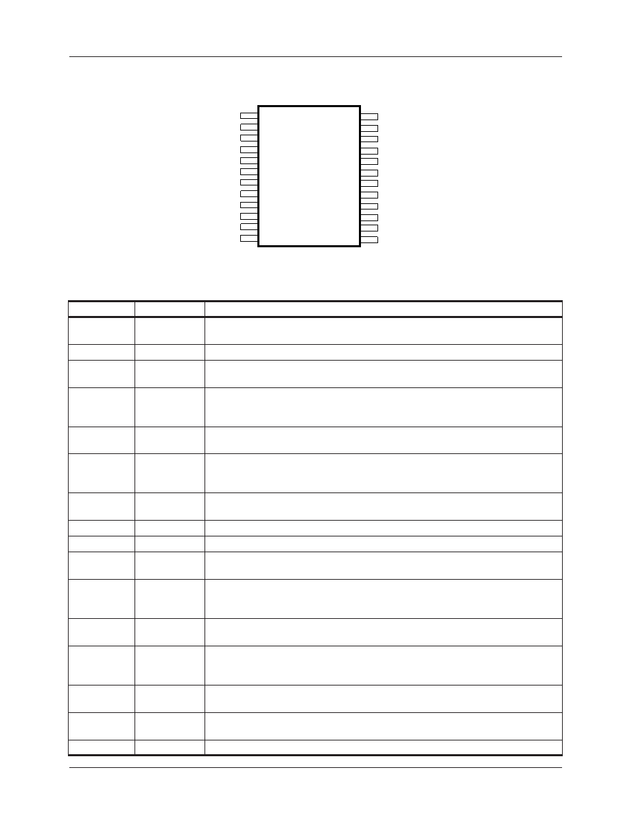
Pin Assignments
Pin Denitions
Pin Number
Pin Name
Pin Function Description
1-5
VID0-4
Voltage Identification Code Inputs. These open collector/TTL compatible
inputs will program the output voltage over the ranges specified in Table 1.
6
BYPASS
5V Rail. Bypass this pin with a 1
F ceramic capacitor to AGND.
7
AGND
Analog Ground. Return path for low power analog circuitry. This pin should be
connected to a low impedance system ground plane to minimize ground loops.
8
LDRVB
Low Side FET Driver for B. Connect this pin to the gate of an N-channel
MOSFET for synchronous operation. The trace from this pin to the MOSFET gate
should be <0.5".
9
PGNDB
Power Ground B. Return pin for high currents flowing in low-side MOSFET.
Connect directly to low-side MOSFET source.
10
SWB
High side driver source and low side driver drain switching node B. Gate
drive return for high side MOSFET, and negative input for low-side MOSFET
current sense.
11
HDRVB
High Side FET Driver B. Connect this pin to the gate of an N-channel MOSFET.
The trace from this pin to the MOSFET gate should be <0.5".
12
BOOTB
Bootstrap B. Input supply for high-side MOSFET.
13
BOOTA
Bootstrap A. Input supply for high-side MOSFET.
14
HDRVA
High Side FET Driver A. Connect this pin to the gate of an N-channel MOSFET.
The trace from this pin to the MOSFET gate should be <0.5".
15
SWA
High side driver source and low side driver drain switching node A. Gate
drive return for high side MOSFET, and negative input for low-side MOSFET
current sense.
16
PGNDA
Power Ground A. Return pin for high currents flowing in low-side MOSFET.
Connect directly to low-side MOSFET source.
17
LDRVA
Low Side FET Driver for A. Connect this pin to the gate of an N-channel
MOSFET for synchronous operation. The trace from this pin to the MOSFET gate
should be <0.5".
18
VCC
VCC. Internal IC supply. Connect to system 12V supply, and decouple with a
0.1
F ceramic capacitor.
19
PWRGD
Power Good Flag. An open collector output that will be logic LOW if the output
voltage is not within +10/-15% of the nominal output voltage setpoint.
20
ILIM
Current Limit. A resistor from this pin to ground sets the over current trip level.
FAN5093
VID0
VID1
VID2
VID3
VID4
AGND
BYPASS
LDRVB
PGNDB
SWB
HDRVB
BOOTB
VFB
RT
ENABLE/SS
DROOP/E*
ILIM
PWRGD
VCC
LDRVA
PGNDA
SWA
HDRVA
BOOTA
1
2
3
4
5
6
7
8
9
10
11
12
24
23
22
21
20
19
18
17
16
15
14
13
相關PDF資料 |
PDF描述 |
|---|---|
| FAN5240MSA | DUAL SWITCHING CONTROLLER, 345 kHz SWITCHING FREQ-MAX, PDSO28 |
| FAN5355MP07X | 1.8 A SWITCHING CONTROLLER, 3350 kHz SWITCHING FREQ-MAX, PDSO10 |
| FAN5355UC07X | 1.8 A SWITCHING CONTROLLER, 3350 kHz SWITCHING FREQ-MAX, PBGA12 |
| FAN5355UC06X | 1.8 A SWITCHING CONTROLLER, 3350 kHz SWITCHING FREQ-MAX, PBGA12 |
| FAN5361UC19X | 0.6 A SWITCHING REGULATOR, 6600 kHz SWITCHING FREQ-MAX, PBGA6 |
相關代理商/技術參數(shù) |
參數(shù)描述 |
|---|---|
| FAN5201 | 制造商:未知廠家 制造商全稱:未知廠家 功能描述: |
| FAN5201MSA | 制造商:未知廠家 制造商全稱:未知廠家 功能描述:Battery Management |
| FAN5230 | 制造商:FAIRCHILD 制造商全稱:Fairchild Semiconductor 功能描述:System Electronics Regulator for Mobile PCs |
| FAN5230_CAC3026B WAF | 制造商:Fairchild Semiconductor Corporation 功能描述: |
| FAN5230QSC | 功能描述:DC/DC 開關控制器 Regulator System Electronics RoHS:否 制造商:Texas Instruments 輸入電壓:6 V to 100 V 開關頻率: 輸出電壓:1.215 V to 80 V 輸出電流:3.5 A 輸出端數(shù)量:1 最大工作溫度:+ 125 C 安裝風格: 封裝 / 箱體:CPAK |
發(fā)布緊急采購,3分鐘左右您將得到回復。