- 您現(xiàn)在的位置:買賣IC網(wǎng) > PDF目錄375725 > FAN5330 (Fairchild Semiconductor Corporation) High Efficiency Serial LED Driver with 30V Integrated Switch PDF資料下載
參數(shù)資料
| 型號: | FAN5330 |
| 廠商: | Fairchild Semiconductor Corporation |
| 元件分類: | LED驅(qū)動器 |
| 英文描述: | High Efficiency Serial LED Driver with 30V Integrated Switch |
| 中文描述: | 高效率串行LED驅(qū)動器30V的集成開關(guān) |
| 文件頁數(shù): | 6/10頁 |
| 文件大?。?/td> | 520K |
| 代理商: | FAN5330 |

6
www.fairchildsemi.com
FAN5330 Rev. 1.0.1
F
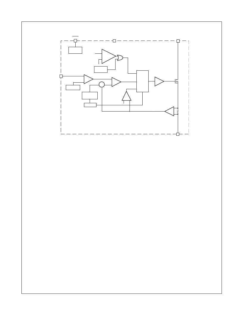
Block Diagram
Figure 4. Block Diagram
Circuit Description
The FAN5330 is a pulse-width modulated (PWM) current-mode
boost converter. The FAN5330 improves the performance of bat-
tery powered equipment by significantly minimizing the spectral
distribution of noise at the input caused by the switching action of
the regulator. In order to facilitate effective noise filtering, the
switching frequency was chosen to be high, 1.5MHz. The device
architecture is that of a current mode controller with an internal
sense resistor connected in series with the N-channel switch.
The voltage at the feedback pin tracks the output voltage at the
cathode of the external Schottky diode (shown in the test cir-
cuit). The error amplifier amplifies the difference between the
feedback voltage and the internal bandgap reference. The
amplified error voltage serves as a reference voltage to the
PWM comparator. The inverting input of the PWM comparator
consists of the sum of two components: the amplified control
signal received from the 30m
current sense resistor and the
ramp generator voltage derived from the oscillator. The oscilla-
tor sets the latch, and the latch turns on the FET switch. Under
normal operating conditions, the PWM comparator resets the
latch and turns off the FET, thus terminating the pulse. Since
the comparator input contains information about the output volt-
age and the control loop is arranged to form a negative feed-
back loop, the value of the peak inductor current will be adjusted
to maintain regulation.
Every time the latch is reset, the FET is turned off and the cur-
rent flow through the switch is terminated. The latch can be
reset by other events as well. Over-current condition is moni-
tored by the current limit comparator which resets the latch and
turns off the switch instantaneously within each clock cycle.
Over-Voltage Protection
The voltage on the feedback pin is sensed by an OVP Compar-
ator. When the feedback voltage is 15% higher than the nominal
voltage, the OVP Comparator stops switching of the power tran-
sistor, thus preventing the output voltage from going higher.
Open-circuit protection
As in any current regulator, if the feedback loop is open, the out-
put voltage increases until it is limited by some additional exter-
nal circuitry. In the particular case of the FAN5330, the output
voltage is limited by the switching transistor breakdown at
around 45V, typically (assuming that C
diode rating voltage are higher). Since at such high output volt-
age the output current is inherently limited by the discontinuous
conduction mode, in most cases, the switching transistor enters
non-destructive breakdown and the IC survives.
OUT
and the Schottky
However, to ensure 100% protection for LED disconnection, we
recommend limiting V
OUT
with an external Zener diode or stop-
ping the boost switching with an external voltage supervisory
circuit.
Applications Information
Setting the Output Current
The internal reference (V
current is set by a resistor divider R connected between FB pin
and ground. The output current is given by
REF
) is 110mV (Typical). The output
Reference
Oscillator
n
FB
FB
+
Driver
Comp
-
Over
Voltage
Comp
-
+
+
Σ
Ramp
Generator
R
R
R
Q
S
Current Limit
Comparator
30m
1.15 x V
REF
Shutdown
Circuitry
Thermal
Shutdown
SHDN
4
GND
SW
1
V
IN
5
Amp
Amp
2
3
+
-
-
+
-
I
LED
V
-----R
=
相關(guān)PDF資料 |
PDF描述 |
|---|---|
| FAN5331 | 1.6MHz Boost Converter with 20V Integrated FET Switch |
| FAN5331SX | 1.6MHz Boost Converter with 20V Integrated FET Switch |
| FAN5332A | High Efficiency, High Current Serial LED Driver and OLED Supply with 30V Integrated Switch |
| FAN5332ASX | High Efficiency, High Current Serial LED Driver and OLED Supply with 30V Integrated Switch |
| FAN5333A | High Efficiency, High Current Serial LED Driver with 30V Integrated Switch |
相關(guān)代理商/技術(shù)參數(shù) |
參數(shù)描述 |
|---|---|
| FAN5330SX | 功能描述:LED照明驅(qū)動器 SYSTEM_POWER RoHS:否 制造商:STMicroelectronics 輸入電壓:11.5 V to 23 V 工作頻率: 最大電源電流:1.7 mA 輸出電流: 最大工作溫度: 安裝風(fēng)格:SMD/SMT 封裝 / 箱體:SO-16N |
| FAN5331 | 制造商:FAIRCHILD 制造商全稱:Fairchild Semiconductor 功能描述:High Efficiency Serial LED Driver and OLED Supply with 20V Integrated Switch |
| FAN5331_05 | 制造商:FAIRCHILD 制造商全稱:Fairchild Semiconductor 功能描述:High Efficiency Serial LED Driver and OLED Supply with 20V Integrated Switch |
| FAN5331_ACC3086B WAF | 制造商:Fairchild Semiconductor Corporation 功能描述: |
| FAN5331SX | 功能描述:LED照明驅(qū)動器 Adj 1.6MHz Boost Reg w/ 25V FET Switch RoHS:否 制造商:STMicroelectronics 輸入電壓:11.5 V to 23 V 工作頻率: 最大電源電流:1.7 mA 輸出電流: 最大工作溫度: 安裝風(fēng)格:SMD/SMT 封裝 / 箱體:SO-16N |
發(fā)布緊急采購,3分鐘左右您將得到回復(fù)。