- 您現(xiàn)在的位置:買賣IC網(wǎng) > PDF目錄375847 > FM25C020U (Fairchild Semiconductor Corporation) 14=2X7 0.1" T/H MALE HDR SN PDF資料下載
參數(shù)資料
| 型號: | FM25C020U |
| 廠商: | Fairchild Semiconductor Corporation |
| 英文描述: | 14=2X7 0.1" T/H MALE HDR SN |
| 中文描述: | 的2K位SPI⑩的CMOS EEPROM的串行接口 |
| 文件頁數(shù): | 1/11頁 |
| 文件大小: | 105K |
| 代理商: | FM25C020U |

1
www.fairchildsemi.com
FM25C020U Rev. B
F
FM25C020U
2K-Bit SPI Interface
Serial CMOS EEPROM
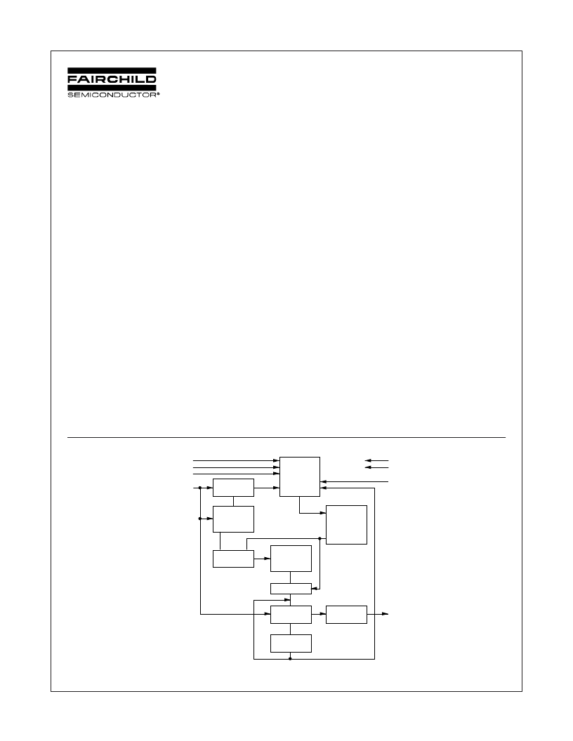
Block Diagram
February 2002
2002 Fairchild Semiconductor Corporation
Instruction
Decoder
Control Logic
and Clock
Generators
High Voltage
Generator
and
Program
Timer
Instruction
Register
Program
Enable
Data In/Out Register
8 Bits
Data Out
Buffer
Non-Volatile
Status Register
Decoder
Address
Counter/
Register
EEPROM Array
Read/Write Amps
/CS
/HOLD
SCK
V
CC
V
SS
V
PP
/WP
SI
SO
General Description
The FM25C020U is a 2K (2,048) bit serial interface CMOS
EEPROM (Electrically Erasable Programmable Read-Only
Memory). This device fully conforms to the SPI 4-wire protocol
which uses Chip Select (/CS), Clock (SCK), Data-in (SI) and Data-
out (SO) pins to synchronously control data transfer between the
SPI microcontroller and the EEPROM. In addition, the serial
interface allows a minimal pin count, packaging designed to
simplify PC board layout requirements and offers the designer a
variety of low voltage and low power options.
This SPI EEPROM family is designed to work with the 68HC11 or
any other SPI-compatible, high-speed microcontroller and offers
both hardware (/WP pin) and software ("block write") data protec-
tion. For example, entering a 2-bit code into the STATUS REGIS-
TER prevents programming in a selected block of memory and all
programming can be inhibited by connecting the /WP pin to V
SS
;
allowing the user to protect the entire array or a selected section.
In addition, SPI devices feature a /HOLD pin, which allows a
temporary interruption of the datastream into the EEPROM.
Fairchild EEPROMs are designed and tested for applications
requiring high endurance, high reliability, and low power con-
sumption for a continuously reliable non-volatile solution for all
markets.
Functions
I
SPI MODE 0 interface
I
2,048 bits organized as 256 x 8
I
Extended 2.7V to 5.5V operating voltage
I
2.1 MHz operation @ 4.5V - 5.5V
I
Self-timed programming cycle
I
"Programming complete" indicated by STATUS REGISTER
polling
I
/WP pin and BLOCK WRITE protection
Features
I
Sequential read of entire array
I
4 byte "Page write" mode to minimize total write time per
byte
I
/WP pin and BLOCK WRITE protection to prevent inadvert-
ent programming as well as programming ENABLE and
DISABLE opcodes.
I
/HOLD pin to suspend data transfer
I
Typical 1
μ
A standby current (I
SB
) for "L" devices and 0.1
μ
A
standby current for "LZ" devices.
I
Endurance: Up to 1,000,000 data changes
I
Data retention greater than 40 years
SPI is a trademark of Motorola Corporation
相關(guān)PDF資料 |
PDF描述 |
|---|---|
| FM25C020UE | LOW PROFILE .025 SQ STRIPS |
| FM25C020UV | CONN-HDR,7P 1ROW,.1SP, TIN, LO PF |
| FM25C040 | The CAT24FC02 is a 2-kb Serial CMOS EEPROM internally organized as 256 words of 8 bits each |
| FM25C040U | LOW PROFILE .025 SQ STRIPS |
| FM25C040UE | CONN,HEADER,2X8,AV,.100 |
相關(guān)代理商/技術(shù)參數(shù) |
參數(shù)描述 |
|---|---|
| FM25C020UE | 制造商:FAIRCHILD 制造商全稱:Fairchild Semiconductor 功能描述:2K-Bit SPI⑩ Interface Serial CMOS EEPROM |
| FM25C020UEM8 | 功能描述:電可擦除可編程只讀存儲器 SOIC-8 RoHS:否 制造商:Atmel 存儲容量:2 Kbit 組織:256 B x 8 數(shù)據(jù)保留:100 yr 最大時(shí)鐘頻率:1000 KHz 最大工作電流:6 uA 工作電源電壓:1.7 V to 5.5 V 最大工作溫度:+ 85 C 安裝風(fēng)格:SMD/SMT 封裝 / 箱體:SOIC-8 |
| FM25C020UEM8X | 功能描述:電可擦除可編程只讀存儲器 DISC BY MFG 7/03 RoHS:否 制造商:Atmel 存儲容量:2 Kbit 組織:256 B x 8 數(shù)據(jù)保留:100 yr 最大時(shí)鐘頻率:1000 KHz 最大工作電流:6 uA 工作電源電壓:1.7 V to 5.5 V 最大工作溫度:+ 85 C 安裝風(fēng)格:SMD/SMT 封裝 / 箱體:SOIC-8 |
| FM25C020UEMT8 | 制造商:未知廠家 制造商全稱:未知廠家 功能描述:SPI Serial EEPROM |
| FM25C020UEN | 制造商:未知廠家 制造商全稱:未知廠家 功能描述:SPI Serial EEPROM |
發(fā)布緊急采購,3分鐘左右您將得到回復(fù)。