- 您現(xiàn)在的位置:買賣IC網 > PDF目錄296013 > FM25C041ULN SPI Serial EEPROM PDF資料下載
參數(shù)資料
| 型號: | FM25C041ULN |
| 英文描述: | SPI Serial EEPROM |
| 中文描述: | SPI串行EEPROM |
| 文件頁數(shù): | 6/11頁 |
| 文件大小: | 101K |
| 代理商: | FM25C041ULN |
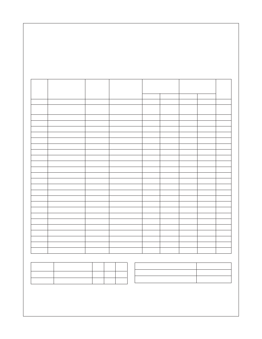
4
www.fairchildsemi.com
FM25C041U
FM25C041U
4K-Bit
SPI
Interface
Serial
CMOS
EEPROM
Low Voltage 2.7V
≤ V
CC ≤ 4.5V Specifications
Absolute Maximum Ratings (Note 5)
Ambient Storage Temperature
-65
°C to +150°C
All Input or Output Voltage with
Respect to Ground
+6.5V to -0.3V
Lead Temp. (Soldering, 10 sec.)
+300
°C
ESD Rating
2000V
Operating Conditions
Ambient Operating Temperature
FM25C041UL/LZ
0
°C to +70°C
FM25C041ULE/LZE
-40
°C to +85°C
FM25C041ULV
-40
°C to +125°C
Power Supply (V
CC)
2.7V–4.5V
DC and AC Electrical Characteristics 2.7V
≤ V
CC ≤ 4.5V (unless otherwise specified)
25C041UL/LE
25C041ULV
25C041ULZ/ZE
Symbol
Parameter
Part
Conditions
Min.
Max.
Min
Max
Units
ICC
Operating Current
/CS = VIL
33
mA
I
CCSB
Standby Current
L
/CS = V
CC
10
A
LZ
1
N/A
A
I
IL
Input Leakage
V
IN = 0 to VCC
-1
1
-1
1
A
I
OL
Output Leakage
V
OUT = GND to VCC
-1
1
-1
1
A
V
IL
Input Low Voltage
-0.3
V
CC * 0.3
-0.3
V
CC * 0.3
V
IH
Input High Voltage
V
CC * 0.7
V
CC + 0.3
V
CC * 0.7
V
CC + 0.3
V
OL
Output Low Voltage
I
OL = 0.8 mA
0.4
V
OH
Output High Voltage
I
OH = –0.8 mA
V
CC - 0.8
V
CC - 0.8
V
f
OP
SCK Frequency
1.0
MHz
t
RI
Input Rise Time
2.0
s
t
FI
Input Fall Time
2.0
s
t
CLH
Clock High Time
(Note 6)
410
ns
t
CLL
Clock Low Time
(Note 6)
410
ns
t
CSH
Min. /CS High Time
(Note 7)
500
ns
t
CSS
/CS Setup Time
500
ns
t
DIS
Data Setup Time
100
ns
t
HDS
/HOLD Setup Time
240
ns
t
CSN
/CS Hold Time
500
ns
t
DIN
Data Hold Time
100
ns
t
HDN
/HOLD Hold Time
240
ns
t
PD
Output Delay
C
L = 200 pF
500
ns
t
DH
Output Hold Time
0
ns
t
LZ
/HOLD Output Low Z
240
ns
t
DF
Output Disable Time
C
L = 200 pF
500
ns
t
HZ
/HOLD to Output Hi Z
240
ns
t
WP
Write Cycle Time
1-16 Bytes
15
ms
Capacitance T
A = 25°C, f = 2.1/1 MHz (Note 8)
Symbol
Test
Typ Max Units
C
OUT
Output Capacitance
3
8
pF
CIN
Input Capacitance
2
6
pF
AC Test Conditions
Output Load
CL = 200pF
Input Pulse Levels
0.1 * V
CC - 0.9 * VCC
Timing Measurement Reference Level
0.3 * VCC - 0.7 * VCC
Note 5: Stress above those listed under “Absolute Maximum Ratings” may cause permanent damage to the device. This is a stress rating only, and functional operation of the device
at these or any other conditions above those indicated in the operational sections of the specification is not implied. Exposure to absolute maximum rating conditions for extended
periods may affect device reliability.
Note 6: The fOP frequency specification specifies a minimum clock period of 1/fOP. Therefore, for every fOP clock cycle, tCLH + tCLL must be equal to or greater than 1/fOP. For
example, for a fOP of 1MHz, the period equals 1000ns. In this case if tCLH = is set to 410ns, then tCLL must be set to a minimum of 590ns.
Note 7: /CS must be brought high for a minimum of tCSH between consecutive instruction cycles.
Note 8: This parameter is periodically sampled and not 100% tested.
相關PDF資料 |
PDF描述 |
|---|---|
| FM25C041ULVMT8 | SPI Serial EEPROM |
| FM25C041ULZEM8 | SPI Serial EEPROM |
| FM25C041ULZEN | SPI Serial EEPROM |
| FM25C041ULZMT8 | SPI Serial EEPROM |
| FMC1819C6-02 | 18700 MHz - 19700 MHz RF/MICROWAVE WIDE BAND LOW POWER AMPLIFIER |
相關代理商/技術參數(shù) |
參數(shù)描述 |
|---|---|
| FM25C041ULVM8 | 制造商:FAIRCHILD 制造商全稱:Fairchild Semiconductor 功能描述:SERIAL EEPROM|512X8|CMOS|SOP|8PIN|PLASTIC |
| FM25C041ULVMT8 | 制造商:未知廠家 制造商全稱:未知廠家 功能描述:SPI Serial EEPROM |
| FM25C041ULVN | 制造商:FAIRCHILD 制造商全稱:Fairchild Semiconductor 功能描述:SERIAL EEPROM|512X8|CMOS|DIP|8PIN|PLASTIC |
| FM25C041ULZEM8 | 制造商:未知廠家 制造商全稱:未知廠家 功能描述:SPI Serial EEPROM |
| FM25C041ULZEMT8 | 制造商:FAIRCHILD 制造商全稱:Fairchild Semiconductor 功能描述:SERIAL EEPROM|512X8|CMOS|TSSOP|8PIN|PLASTIC |
發(fā)布緊急采購,3分鐘左右您將得到回復。