- 您現(xiàn)在的位置:買賣IC網(wǎng) > PDF目錄370207 > FM31256 4Kb FRAM Serial 3V Memory PDF資料下載
參數(shù)資料
| 型號: | FM31256 |
| 元件分類: | F-RAM |
| 英文描述: | 4Kb FRAM Serial 3V Memory |
| 中文描述: | 4Kb的鐵電串行3V的記憶 |
| 文件頁數(shù): | 3/22頁 |
| 文件大?。?/td> | 170K |
| 代理商: | FM31256 |

FM3104/16/64/256
Rev 0.21
Nov 2003
Page 3 of 22
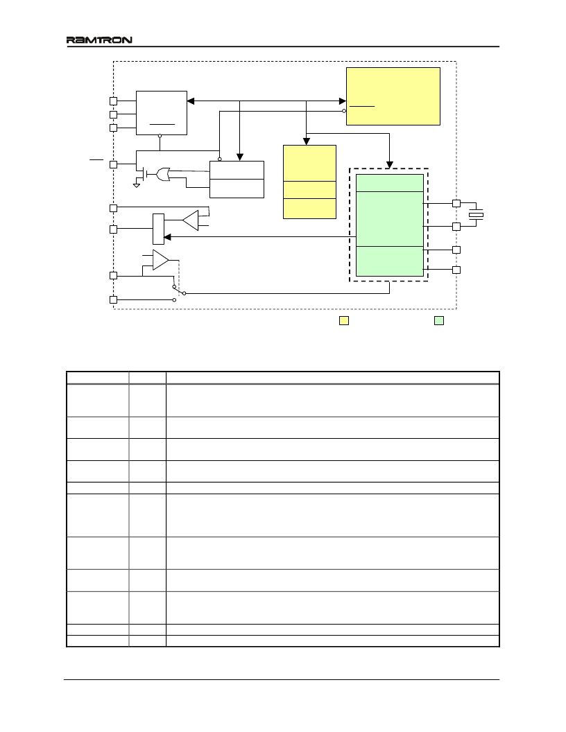
Figure 1. Block Diagram
Pin Descriptions
Pin Name
A0, A1
Type
Input
Pin Description
Device select inputs are used to address multiple memories on a serial bus. To select
the device the address value on the two pins must match the corresponding bits
contained in the device address. The device select pins are pulled down internally.
Event Counter Inputs: These battery-backed inputs increment counters when an edge is
detected on the corresponding CNT pin. The polarity is programmable.
In calibration mode, this pin supplies a 512 Hz square-wave output for clock
calibration. In normal operation, this is the early power-fail output.
32.768 kHz crystal connection. When using an external oscillator, apply the clock to
X2 and leave X1 floating.
Active low reset output with weak pull-up. Also input for manual reset.
Serial Data & Address: This is a bi-directional line for the two-wire interface. It is
open-drain and is intended to be wire-OR’d with other devices on the two-wire bus.
The input buffer incorporates a Schmitt trigger for noise immunity and the output
driver includes slope control for falling edges. A pull-up resistor is required.
Serial Clock: The serial clock line for the two-wire interface. Data is clocked out of the
part on the falling edge, and in on the rising edge. The SCL input also incorporates a
Schmitt trigger input for noise immunity.
Early Power-fail Input: Typically connected to an unregulated power supply to detect
an early power failure. This pin should not be left floating.
Backup supply voltage: A 3V battery or a large value capacitor. If V
DD
<3.6V and no
backup supply is used, this pin should be tied to V
DD
. If V
DD
>3.6V and no backup
supply is used, this pin should be left floating and the VBC bit should be set.
Supply Voltage.
Ground
CNT1, CNT2
Input
CAL/PFO
Output
X1, X2
I/O
/RST
SDA
I/O
I/O
SCL
Input
PFI
Input
VBAK
Supply
VDD
VSS
Supply
Supply
FRAM
Array
2-Wire
Interface
SCL
SDA
RST
A1, A0
CAL/PFO
PFI
VDD
VBAK
RTC
2.5V
-
+
RTC Registers
Event
Counters
CNT1
CNT2
Special
Function
Registers
S/N
X1
X2
LockOut
LockOut
+
-
1.2V
Watchdog
LV Detect
Switched Power
512Hz
RTC Cal.
Battery Backed
Nonvolatile
相關(guān)PDF資料 |
PDF描述 |
|---|---|
| FM320B | SURFACE MOUNT SCHOTTKY BARRIER RECTIFIER VOLTAGE RANGE 20 to 60 Volts CURRENT 3.0 Amperes |
| FM330B | SURFACE MOUNT SCHOTTKY BARRIER RECTIFIER VOLTAGE RANGE 20 to 60 Volts CURRENT 3.0 Amperes |
| FM340B | SURFACE MOUNT SCHOTTKY BARRIER RECTIFIER VOLTAGE RANGE 20 to 60 Volts CURRENT 3.0 Amperes |
| FM350B | SURFACE MOUNT SCHOTTKY BARRIER RECTIFIER VOLTAGE RANGE 20 to 60 Volts CURRENT 3.0 Amperes |
| FM360B | SURFACE MOUNT SCHOTTKY BARRIER RECTIFIER VOLTAGE RANGE 20 to 60 Volts CURRENT 3.0 Amperes |
相關(guān)代理商/技術(shù)參數(shù) |
參數(shù)描述 |
|---|---|
| FM31256_11 | 制造商:RAMTRON 制造商全稱:RAMTRON 功能描述:Integrated Processor Companion with Memory |
| FM31256-G | 功能描述:監(jiān)控電路 256K w/RTC Pwr Mon WDT Bat Sw PF RoHS:否 制造商:STMicroelectronics 監(jiān)測電壓數(shù): 監(jiān)測電壓: 欠電壓閾值: 過電壓閾值: 輸出類型:Active Low, Open Drain 人工復(fù)位:Resettable 監(jiān)視器:No Watchdog 電池備用開關(guān):No Backup 上電復(fù)位延遲(典型值):10 s 電源電壓-最大:5.5 V 最大工作溫度:+ 85 C 安裝風(fēng)格:SMD/SMT 封裝 / 箱體:UDFN-6 封裝:Reel |
| FM31256-G | 制造商:Ramtron International Corporation 功能描述:Voltage Detector / Microprocessor Superv |
| FM31256-GTR | 功能描述:監(jiān)控電路 256K w/RTC Pwr Mon WDT Bat Sw PF RoHS:否 制造商:STMicroelectronics 監(jiān)測電壓數(shù): 監(jiān)測電壓: 欠電壓閾值: 過電壓閾值: 輸出類型:Active Low, Open Drain 人工復(fù)位:Resettable 監(jiān)視器:No Watchdog 電池備用開關(guān):No Backup 上電復(fù)位延遲(典型值):10 s 電源電壓-最大:5.5 V 最大工作溫度:+ 85 C 安裝風(fēng)格:SMD/SMT 封裝 / 箱體:UDFN-6 封裝:Reel |
| FM31256-S | 功能描述:監(jiān)控電路 256K w/RTC Pwr Mon WDT Bat Sw PF RoHS:否 制造商:STMicroelectronics 監(jiān)測電壓數(shù): 監(jiān)測電壓: 欠電壓閾值: 過電壓閾值: 輸出類型:Active Low, Open Drain 人工復(fù)位:Resettable 監(jiān)視器:No Watchdog 電池備用開關(guān):No Backup 上電復(fù)位延遲(典型值):10 s 電源電壓-最大:5.5 V 最大工作溫度:+ 85 C 安裝風(fēng)格:SMD/SMT 封裝 / 箱體:UDFN-6 封裝:Reel |
發(fā)布緊急采購,3分鐘左右您將得到回復(fù)。