- 您現(xiàn)在的位置:買賣IC網(wǎng) > PDF目錄375863 > FMS6246 (Fairchild Semiconductor Corporation) Six Channel, 6th Order SD/PS Video Filter Driver PDF資料下載
參數(shù)資料
| 型號(hào): | FMS6246 |
| 廠商: | Fairchild Semiconductor Corporation |
| 英文描述: | Six Channel, 6th Order SD/PS Video Filter Driver |
| 中文描述: | 六通道6階標(biāo)清/聚苯乙烯視頻濾波驅(qū)動(dòng)器 |
| 文件頁(yè)數(shù): | 6/10頁(yè) |
| 文件大小: | 92K |
| 代理商: | FMS6246 |

6
www.fairchildsemi.com
FMS6246 Rev. 1A
F
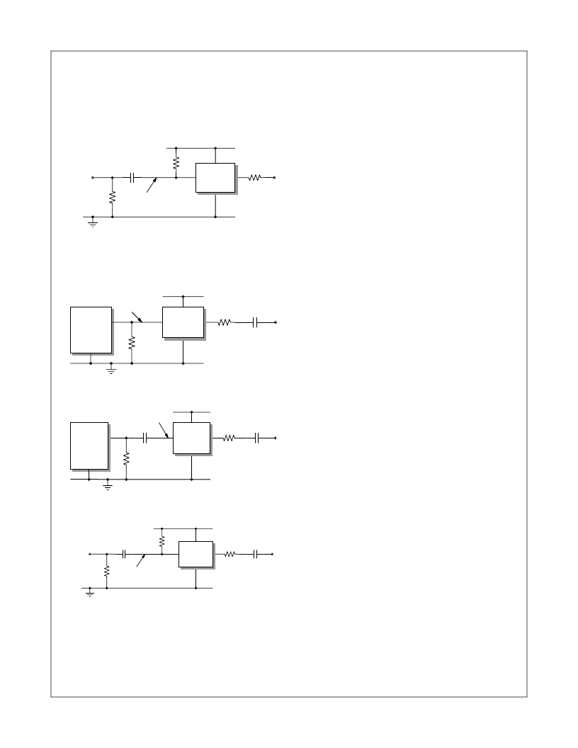
The same method can be used for biased signals with the addi-
tion of a pull-up resistor to make sure the clamp never operates.
The internal pull-down resistance is 800k
±20% so the exter-
nal resistance should be 7.5M
to set the DC level to 500mV. If
a pull-up resistance less than 7.5M
is desired, an external
pull-down can be added such that the DC input level is set to
500mV.
Figure 6.
Biased SCART with DC-coupled Outputs
The same circuits can be used with AC-coupled outputs if
desired.
Figure 7. DC-coupled inputs, AC-coupled Outputs
Figure 8.
AC-coupled inputs and outputs
Figure 9.
Biased SCART with AC-Coupled Outputs
NOTE: The video tilt or line time distortion will be dominated by
the AC-coupling capacitor. The value may need to be increased
beyond 220uF in order to obtain satisfactory operation in some
applications.
Power Dissipation
The FMS6246 output drive configuration must be considered
when calculating overall power dissipation. Care must be taken
not to exceed the maximum die junction temperature. The fol-
lowing example can be used to calculate the FMS6246’s power
dissipation and internal temperature rise.
T
j
= T
A
+ P
d
Θ
JA
where P
d
= P
CH1
+ P
CH2
+ P
CHx
and P
CHx
= V
s
I
CH
- (V
O2
/R
L
)
where
V
O
= 2V
in
+ 0.280V
I
CH
= (I
CC
/ 6) + (V
O
/R
L
)
V
in
= RMS value of input signal
I
CC
= 60mA
V
s
= 5V
R
L
= channel load resistance
Board layout can also affect thermal characteristics. Refer to the
Layout Considerations
Section for more information.
Layout Considerations
General layout and supply bypassing play major roles in high
frequency performance and thermal characteristics. Fairchild
offers a demonstration board, FMS6246DEMO, to use as a
guide for layout and to aid in device testing and characterization.
The FMS6246DEMO is a 4-layer board with a full power and
ground plane. Following this layout configuration will provide the
optimum performance and thermal characteristics. For optimum
results, follow the steps below as a basis for high frequency lay-
out:
Include 10
μ
F and 0.1
μ
F ceramic bypass capacitors
Place the 10
μ
F capacitor within 0.75 inches of the power pin
Place the 0.1
μ
F capacitor within 0.1 inches of the power pin
For multi-layer boards, use a large ground plane to help dissi-
pate heat
For 2 layer boards, use a ground plane that extends beyond
the device by at least 0.5”
Minimize all trace lengths to reduce series inductances
75
LCVF
Bias
Input
75
0.1u
External Video
source must
be AC-coupled.
500mV +/-350mV
7.5M
DVD or
STB
SoC
DAC
Output
75
LCVF
Clamp
Inactive
0V - 1.4V
220u
75
LCVF
Clamp
Active
0.1u
0V - 1.4V
220u
DVD or
STB
SoC
DAC
Output
75
LCVF
Clamp
Active
75
0.1u
External video
source must
be AC-coupled.
220u
500mV +/-350mV
7.5M
相關(guān)PDF資料 |
PDF描述 |
|---|---|
| FMS6246-9 | Six Channel, 6th Order SD/PS Video Filter Driver |
| FMS6246MTC20 | Six Channel, 6th Order SD/PS Video Filter Driver |
| FMS6246MTC20X | Six Channel, 6th Order SD/PS Video Filter Driver |
| FMS6346 | Six Channel, 6th Order SD/HD Video Filter Driver |
| FMS6346-9 | Six Channel, 6th Order SD/HD Video Filter Driver |
相關(guān)代理商/技術(shù)參數(shù) |
參數(shù)描述 |
|---|---|
| FMS6246_06 | 制造商:FAIRCHILD 制造商全稱:Fairchild Semiconductor 功能描述:Six Channel, 6th Order SD/PS Video Filter Driver |
| FMS6246-9 | 制造商:FAIRCHILD 制造商全稱:Fairchild Semiconductor 功能描述:Six Channel, 6th Order SD/PS Video Filter Driver |
| FMS6246MTC20 | 功能描述:視頻 IC Ang fg 6Chanl 6thOrd SD/PSVidFiltrDr RoHS:否 制造商:Fairchild Semiconductor 工作電源電壓:5 V 電源電流:80 mA 最大工作溫度:+ 85 C 封裝 / 箱體:TSSOP-28 封裝:Reel |
| FMS6246MTC209 | 制造商:FAIRCHILD 制造商全稱:Fairchild Semiconductor 功能描述:Six Channel, 6th Order SD/PS Video Filter Driver |
| FMS6246MTC20X | 功能描述:視頻 IC Ang fg 6Chanl 6thOrd SD/PSVidFiltrDr RoHS:否 制造商:Fairchild Semiconductor 工作電源電壓:5 V 電源電流:80 mA 最大工作溫度:+ 85 C 封裝 / 箱體:TSSOP-28 封裝:Reel |
發(fā)布緊急采購(gòu),3分鐘左右您將得到回復(fù)。