- 您現(xiàn)在的位置:買賣IC網(wǎng) > PDF目錄375864 > FMS6408-10 (Fairchild Semiconductor Corporation) Triple Video Filter Driver for RGB and YUV Signals PDF資料下載
參數(shù)資料
| 型號(hào): | FMS6408-10 |
| 廠商: | Fairchild Semiconductor Corporation |
| 英文描述: | Triple Video Filter Driver for RGB and YUV Signals |
| 中文描述: | 三視頻濾波驅(qū)動(dòng)的RGB和YUV信號(hào) |
| 文件頁(yè)數(shù): | 7/9頁(yè) |
| 文件大小: | 250K |
| 代理商: | FMS6408-10 |

REV. 2C August 31, 2004
7
FMS6408
DATA SHEET
+5V
V
CC
YOUT
UOUT
VOUT
75
75
Video Cables
75
75
75
75
75
75
75
75
75
75
75
Driver
Driver
Driver
IY
IU
IV
+ VIY -
+ VIU -
+ VIV -
0.25V
0.85V
1.55V
2.25V
0.425V
1.125V
1.825V
0.425V
1.125V
1.825V
Application Notes
Output Drive Capability
The FMS6408 can drive dual 75
loads where each load
consists of a 75
resistor in series with a 75
termination
resistor in the driven device. This presents a 150
load to
the output so two similar loads in parallel look like 75
from
the output to ground. In some cases it may be desirable to
drive a single load on one or more outputs with a dual load
on the remaining outputs. This is an acceptable loading con-
dition but might cause a slight degradation in gain matching.
Device Power Dissipation
The FMS6408 specifications provide a quiescent no-load
supply current of 52mA (typical). With a nominal 5V
supply, this results in a power dissipation of 260mW. The
overall power dissipation can be significantly affected by the
applied load, particularly in DC-coupled applications. In
order to calculate the total power dissipation the typical
output voltages and the loading must be known.
The highest power dissipation will occur for YUV video sig-
nals that are DC-coupled into dual video loads. Refer to the
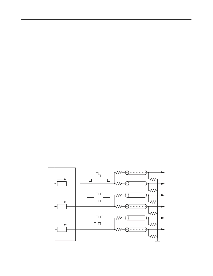
the diagram in Figure 3 below.
Assume a video signal on the Y channel that averages 50%
luminance with an output voltage of 1.55V then calculate the
load current:
I
load
(Y) = 1.55V/75
= 20.6mA
The device dissipation due to this load will be the internal
voltage drop multiplied by the load current:
P
diss
(Y) = (5V - 1.55V) * 20.6mA = 71mW
The average DC level for the U and V channels is set by the
clamp circuit to 1.125V. The signal will be symmetrical
about this voltage so:
I
load
(U) = 1.125V/75
= 15mA
The device dissipation due to this load will be the internal
voltage drop multiplied by the load current:
P
diss
(U) = (5V - 1.125V) * 15mA = 58.125mW
Since the U and V power dissipation are approximately the
same, the total dissipation due to the load can be estimated
by:
P
diss
(load) = P (Y) + 2 * P (U) = 71mW +
(2 * 58.125mW) = 187.55mW
This will bring the typical total device power dissipation to
260mW (quiescent power) + 187.55mW (load power) or
447.55mW. It is advisable to calculate the highest possible
power dissipation using worst-case quiescent supply current
and the maximum allowable power supply voltage. This
result should be used when calculating the die temperature
rise with the supplied
θ
JA
, thermal resistance value.
Field Time Distortion
In applications with AC-coupled outputs, the AC-coupling
capacitors will dominate the field time distortion. Perfor-
mance is specified with 220
μ
F coupling capacitors; if better
performance is desired, the capacitors may be increased or
the outputs may be DC-coupled.
Figure 3. YUV Video Signals that are DC-Coupled into Dual Video Loads
相關(guān)PDF資料 |
PDF描述 |
|---|---|
| FMS6408-11 | Triple Video Filter Driver for RGB and YUV Signals |
| FMS6408-12 | Triple Video Filter Driver for RGB and YUV Signals |
| FMS6408-2 | Triple Video Filter Driver for RGB and YUV Signals |
| FMS6408-3 | Triple Video Filter Driver for RGB and YUV Signals |
| FMS6408-4 | Triple Video Filter Driver for RGB and YUV Signals |
相關(guān)代理商/技術(shù)參數(shù) |
參數(shù)描述 |
|---|---|
| FMS6408-11 | 制造商:FAIRCHILD 制造商全稱:Fairchild Semiconductor 功能描述:Triple Video Filter Driver for RGB and YUV Signals |
| FMS6408-12 | 制造商:FAIRCHILD 制造商全稱:Fairchild Semiconductor 功能描述:Triple Video Filter Driver for RGB and YUV Signals |
| FMS6408-2 | 制造商:FAIRCHILD 制造商全稱:Fairchild Semiconductor 功能描述:Triple Video Filter Driver for RGB and YUV Signals |
| FMS6408-3 | 制造商:FAIRCHILD 制造商全稱:Fairchild Semiconductor 功能描述:Triple Video Filter Driver for RGB and YUV Signals |
| FMS64083_AAB3026B WAF | 制造商:Fairchild Semiconductor Corporation 功能描述: |
發(fā)布緊急采購(gòu),3分鐘左右您將得到回復(fù)。