- 您現(xiàn)在的位置:買(mǎi)賣(mài)IC網(wǎng) > PDF目錄67505 > FMS9875KGC140X (FAIRCHILD SEMICONDUCTOR CORP) 3-CH 8-BIT PROPRIETARY METHOD ADC, PARALLEL ACCESS, PQFP100 PDF資料下載
參數(shù)資料
| 型號(hào): | FMS9875KGC140X |
| 廠商: | FAIRCHILD SEMICONDUCTOR CORP |
| 元件分類(lèi): | ADC |
| 英文描述: | 3-CH 8-BIT PROPRIETARY METHOD ADC, PARALLEL ACCESS, PQFP100 |
| 封裝: | MQFP-100 |
| 文件頁(yè)數(shù): | 4/31頁(yè) |
| 文件大小: | 517K |
| 代理商: | FMS9875KGC140X |
第1頁(yè)第2頁(yè)第3頁(yè)當(dāng)前第4頁(yè)第5頁(yè)第6頁(yè)第7頁(yè)第8頁(yè)第9頁(yè)第10頁(yè)第11頁(yè)第12頁(yè)第13頁(yè)第14頁(yè)第15頁(yè)第16頁(yè)第17頁(yè)第18頁(yè)第19頁(yè)第20頁(yè)第21頁(yè)第22頁(yè)第23頁(yè)第24頁(yè)第25頁(yè)第26頁(yè)第27頁(yè)第28頁(yè)第29頁(yè)第30頁(yè)第31頁(yè)
PRODUCT SPECIFICATION
FMS9875
12
REV. 1.2.15 1/14/02
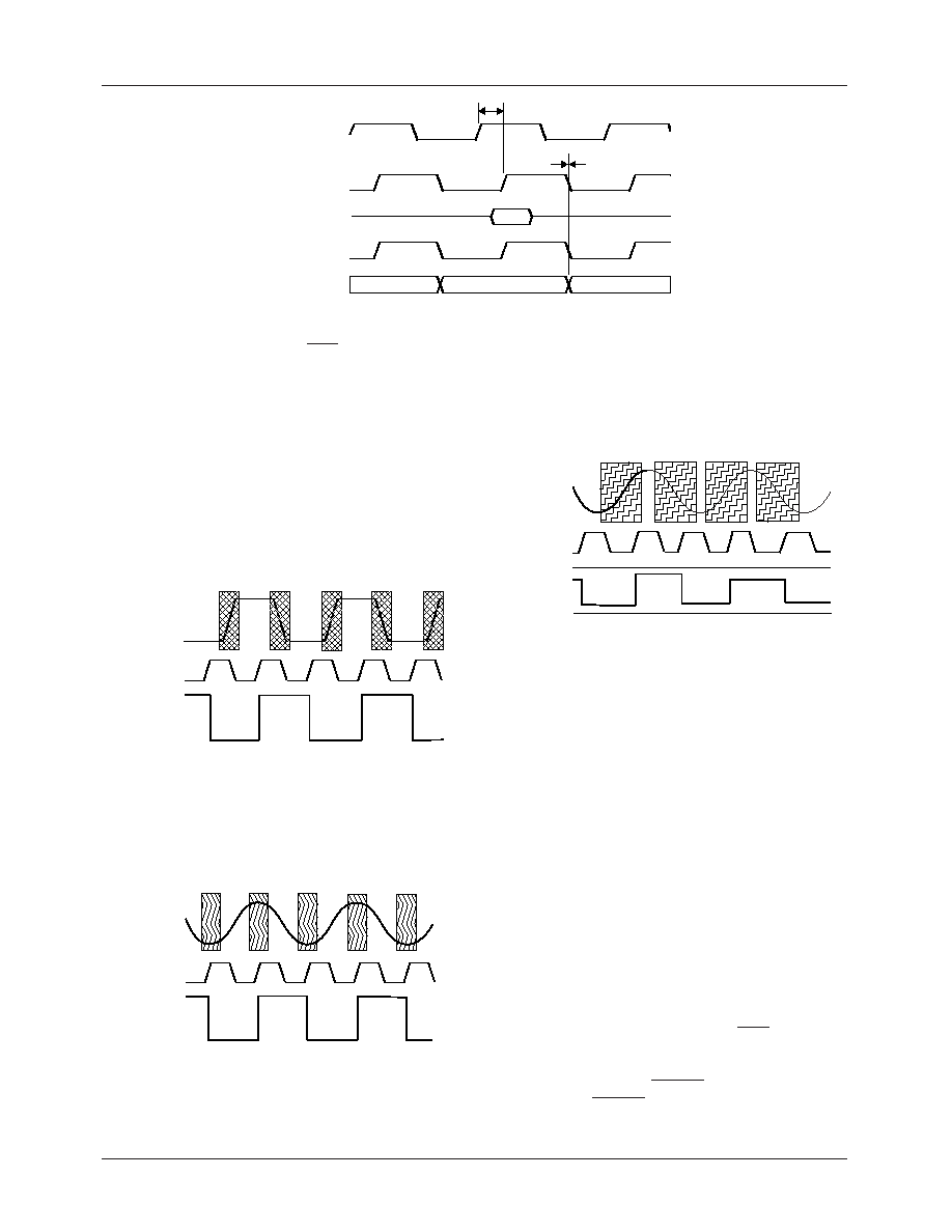
Output data and clocks: DCK and DCK are delayed in tan-
dem with SCK relative to PXCK or XCK. There is a 5-51/2
clock latency between the data sample Sn and the corre-
sponding data out DA7-0.
Ideally, incoming pixels (PC generated) would be trape-
zoidal with fast rise-times and the sampling edge of the A/D
clock, SCK would be positioned along the level section of
the incoming pixel waveform as shown in Figure 4. There is
a narrow zone of uncertainly where sampling during pixel
rise time would cause an error in the value of the A/D data
output, D7-0, which is shown as a value, 0-255.
Figure 4. Ideal Pixel Sampling
In practice, high-resolution pixels have relatively long rise-
times. As shown in Figure 5, there are narrow zones of seren-
dipity when the pixel amplitude is level. Samples are valid in
these zones.
Figure 5. Acceptable Pixel Sampling
Referring to Figure 6, when the sample clock, SCK has some
jitter, if the sampling edge occurs anywhere within the zone
of uncertainty where the pixel rise time is steep, there will be
amplitude modulation of the digitized data, D7-0, due to the
sampling clock jitter. To avoid corruption of the image, set-
ting the value PHASE7-0 is critical. PHASE4-0 should be
trimmed to position the sampling edge of SCK within the
zone of serendipity.
Figure 6. Improper Pixel Sampling
Voltage References
An on-chip voltage reference is generated from a bandgap
source. VREFOUT is the buffered output of this source that
can be connected to VREFIN to supply a voltage reference
that is common to the three converter channels.
VREFIN, with a nominal voltage of 1.25V, is the source of the
differential reference voltages for each A/D converter.
Reference voltages supplied to the differential inputs of the
comparators in the A/D converters are derived from VREFIN.
Digital Data Outputs
Input horizontal sync HSIN and outgoing data, D[7..0] are
resynchronized to the internal delayed sample clock, SCK.
Output timing relationships are dened in Figure 7. Latency of
the rst pixel, N varies according to the mode:
1.
Normal.
2.
Alternate pixel sampling.
Data transitions on the falling edge of the DCK clock. Pixel
data should be sampled on the rising edge of the DCK clock.
Levels are 3.3 volt CMOS. PWRDN = L sets the outputs
high-impedance. PWRDN = H enables the outputs.
D7-0
RIN, GIN, BIN
SCK
Zones of Uncertainty
D7-0
RIN, GIN, BIN
SCK
Zones of Serendipity
D7-0
RIN, GIN, BIN
SCK
Zones of Uncertainty
Figure 3. Internal Sampling Clock, SCK Timing
PHASE
Sn
PXCK/XCK
SCK
VIN
DCK
DA
相關(guān)PDF資料 |
PDF描述 |
|---|---|
| FN3410-10-44 | 500 V, 50 HZ, THREE PHASE EMI FILTER |
| FN3410-110-35 | 500 V, 50 HZ, THREE PHASE EMI FILTER |
| FN3410-13-44 | 500 V, 50 HZ, THREE PHASE EMI FILTER |
| FN3410-150-40 | 500 V, 50 HZ, THREE PHASE EMI FILTER |
| FN3410-16-44 | 500 V, 50 HZ, THREE PHASE EMI FILTER |
相關(guān)代理商/技術(shù)參數(shù) |
參數(shù)描述 |
|---|---|
| FMS9875KWC | 制造商:Fairchild Semiconductor Corporation 功能描述: |
| FMS9884A | 制造商:FAIRCHILD 制造商全稱(chēng):Fairchild Semiconductor 功能描述:3x8-Bit, 108/140/175 Ms/s Triple Video A/D Converter with Clamps |
| FMS9884AKAC100 | 功能描述:視頻模擬/數(shù)字化轉(zhuǎn)換器集成電路 MQFP RoHS:否 制造商:Texas Instruments 輸入信號(hào)類(lèi)型:Differential 轉(zhuǎn)換器數(shù)量:1 ADC 輸入端數(shù)量:4 轉(zhuǎn)換速率:3 Gbps 分辨率:8 bit 結(jié)構(gòu): 輸入電壓:3.3 V 接口類(lèi)型:SPI 信噪比: 電壓參考: 電源電壓-最大:3.45 V 電源電壓-最小:3.15 V 最大功率耗散: 最大工作溫度:+ 85 C 最小工作溫度:- 40 C 封裝 / 箱體:TCSP-48 封裝:Reel |
| FMS9884AKAC140 | 功能描述:視頻模擬/數(shù)字化轉(zhuǎn)換器集成電路 MQFP RoHS:否 制造商:Texas Instruments 輸入信號(hào)類(lèi)型:Differential 轉(zhuǎn)換器數(shù)量:1 ADC 輸入端數(shù)量:4 轉(zhuǎn)換速率:3 Gbps 分辨率:8 bit 結(jié)構(gòu): 輸入電壓:3.3 V 接口類(lèi)型:SPI 信噪比: 電壓參考: 電源電壓-最大:3.45 V 電源電壓-最小:3.15 V 最大功率耗散: 最大工作溫度:+ 85 C 最小工作溫度:- 40 C 封裝 / 箱體:TCSP-48 封裝:Reel |
| FMS9884AKAC175 | 功能描述:視頻模擬/數(shù)字化轉(zhuǎn)換器集成電路 MQFP RoHS:否 制造商:Texas Instruments 輸入信號(hào)類(lèi)型:Differential 轉(zhuǎn)換器數(shù)量:1 ADC 輸入端數(shù)量:4 轉(zhuǎn)換速率:3 Gbps 分辨率:8 bit 結(jié)構(gòu): 輸入電壓:3.3 V 接口類(lèi)型:SPI 信噪比: 電壓參考: 電源電壓-最大:3.45 V 電源電壓-最小:3.15 V 最大功率耗散: 最大工作溫度:+ 85 C 最小工作溫度:- 40 C 封裝 / 箱體:TCSP-48 封裝:Reel |
發(fā)布緊急采購(gòu),3分鐘左右您將得到回復(fù)。