- 您現(xiàn)在的位置:買賣IC網(wǎng) > PDF目錄375865 > FN4819 (Intersil Corporation) Synchronous-Rectified Buck MOSFET Drivers PDF資料下載
參數(shù)資料
| 型號(hào): | FN4819 |
| 廠商: | Intersil Corporation |
| 英文描述: | Synchronous-Rectified Buck MOSFET Drivers |
| 中文描述: | 同步整流降壓MOSFET驅(qū)動(dòng)器 |
| 文件頁(yè)數(shù): | 4/8頁(yè) |
| 文件大?。?/td> | 84K |
| 代理商: | FN4819 |

4
Functional Pin Description
UGATE (Pin 1)
Upper gate drive output. Connect to gate of high-side power
N-Channel MOSFET.
BOOT (Pin 2)
Floating bootstrap supply pin for the upper gate drive.
Connect the bootstrap capacitor between this pin and the
PHASE pin. The bootstrap capacitor provides the charge to
turn on the upper MOSFET. See the Internal Bootstrap
Device section under DESCRIPTION for guidance in
choosing the appropriate capacitor value.
PWM (Pin 3)
The PWM signal is the control input for the driver. The PWM
signal can enter three distinct states during operation, see the
three-statePWMInputsectionunderDESCRIPTIONforfurther
details. Connect this pin to the PWM output of the controller.
GND (Pin 4)
Bias and reference ground. All signals are referenced to this
node.
LGATE (Pin 5)
Lower gate drive output. Connect to gate of the low-side
power N-Channel MOSFET.
VCC (Pin 6)
Connect this pin to a +12V bias supply. Place a high quality
bypass capacitor from this pin to GND.
PVCC (Pin 7)
For the HIP6601, this pin supplies the upper gate drive bias.
Connect this pin from +12V down to +5V.
For the HIP6603, this pin supplies both the upper and lower
gate drive bias. Connect this pin to either +12V or +5V.
PHASE (Pin 8)
Connect this pin to the source of the upper MOSFET and the
drain of the lower MOSFET. The PHASE voltage is
monitored for adaptive shoot-through protection. This pin
also provides a return path for the upper gate drive.
Description
Operation
Designed for versatility and speed, the HIP6601 and HIP6603
dual MOSFET drivers control both high-side and low-side N-
Channel FETs from one externally provided PWM signal.
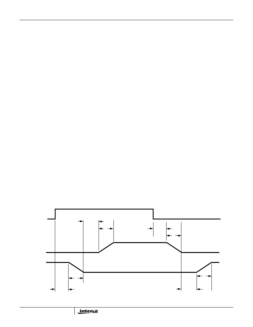
The upper and lower gates are held low until the driver is
initialized. Once the VCC voltage surpasses the VCC Rising
Threshold (See Electrical Specifications), the PWM signal
takes control of gate transitions. A rising edge on PWM
initiates the turn-off of the lower MOSFET (see Timing
Diagram). After a short propagation delay [TPDL
LGATE
], the
lower gate begins to fall. Typical fall times [TF
LGATE
] are
provided in the Electrical Specifications section. Adaptive
shoot-through circuitry monitors the LGATE voltage and
determines the upper gate delay time [TPDH
UGATE
] based
on how quickly the LGATE voltage drops below 1.0V. This
prevents both the lower and upper MOSFETs from
conducting simultaneously or shoot-through. Once this delay
period is complete the upper gate drive begins to rise
[TR
UGATE
] and the upper MOSFET turns on.
Timing Diagram
PWM
UGATE
LGATE
TPDL
LGATE
TF
LGATE
TPDH
UGATE
TR
UGATE
TPDL
UGATE
TF
UGATE
TPDH
LGATE
TR
LGATE
HIP6601, HIP6603
相關(guān)PDF資料 |
PDF描述 |
|---|---|
| FN4819.1 | Synchronous-Rectified Buck MOSFET Drivers |
| FN4871 | Multiple Linear Power Controller with ACPI Control Interface |
| FN561 | OBSOLETE PRODUCT NO RECOMMENDED REPLACEMENT |
| FN6094 | Ultra Low ON-Resistance, Low Voltage, Single Supply, Quad SPDT (Dual DPDT) Analog Switch |
| FN7173 | Sync Separator, 50% Slice, S-H, Filter, Horizontal sync output |
相關(guān)代理商/技術(shù)參數(shù) |
參數(shù)描述 |
|---|---|
| FN4819.1 | 制造商:INTERSIL 制造商全稱:Intersil Corporation 功能描述:Synchronous-Rectified Buck MOSFET Drivers |
| FN4856 | 制造商:Vishay Siliconix 功能描述:FN4856 - Bulk |
| FN4871 | 制造商:INTERSIL 制造商全稱:Intersil Corporation 功能描述:Multiple Linear Power Controller with ACPI Control Interface |
| FN48B3 031392 | 制造商:Comair Rotron 功能描述:FAN 92X92X25MM 48VDC |
| FN48K3 039286 | 制造商:Comair Rotron 功能描述:FAN 92X92X25MM 48VDC |
發(fā)布緊急采購(gòu),3分鐘左右您將得到回復(fù)。