- 您現(xiàn)在的位置:買賣IC網(wǎng) > PDF目錄375914 > FS6051 (Electronic Theatre Controls, Inc.) LOW-SKEW CLOCK FANOUT BUFFER ICs PDF資料下載
參數(shù)資料
| 型號: | FS6051 |
| 廠商: | Electronic Theatre Controls, Inc. |
| 英文描述: | LOW-SKEW CLOCK FANOUT BUFFER ICs |
| 中文描述: | 低偏移時鐘扇出緩沖器集成電路 |
| 文件頁數(shù): | 19/19頁 |
| 文件大?。?/td> | 386K |
| 代理商: | FS6051 |

XT
April 1999
4.5.99
19
)6)6)6)6
/RZ6NHZ&ORFN)DQRXW%XIIHU,&V
,62
Series termination adds no dc loading to the driver, and
requires less power than other resistive termination
methods. Further, no extra impedance exists from the
signal line to a reference voltage, such as ground.
As shown in Figure 19
, the sum of the driver’s output im-
pedance (z
O
) and the series termination resistance (R
S
)
must equal the line impedance (z
L
). That is,
z
R
=
O
L
S
z
.
Note that when the source impedance (z
O
+R
S
) is
matched to the line impedance, then by voltage division
the incident wave amplitude is one-half of the full signal
amplitude.
(
R
z
O
+
The full signal amplitude may take up to twice as long as
the propagation delay of the line to develop, reducing
noise immunity during the half-amplitude period. Note
also that the voltage at the receive end must add up to a
signal amplitude that meets the receiver switching
thresholds. The slew rate of the signal is also reduced
due to the additional RC delay of the load capacitance
and the line impedance. Also note that the output driver
impedance will vary slightly with the output logic state
(high or low).
2
)
(
)
V
z
R
z
V
V
L
S
S
+
O
i
=
+
=
8.2
High-speed clock drivers require careful attention to
power dissipation. Transient power (P
T
) consumption can
be derived from
×
=
Dynamic Power Dissipation
SW
CLK
load
DD
T
N
f
C
V
P
×
×
2
where C
load
is the load capacitance, V
DD
is the supply
voltage, f
CLK
is the clock frequency, and N
sw
is the
number of switching outputs.
The internal heat (junction temperature, T
J
) generated by
the power dissipation can be calculated from
T
Θ
=
where
Θ
JA
is the package thermal resistance, T
A
is the
ambient temperature, and P
T
is derived above.
A
T
JA
J
T
P
+
×
8.3
Connection of devices to a standard-mode implementa-
tion of either the I
2
C-bus or the SMBus is similar to that
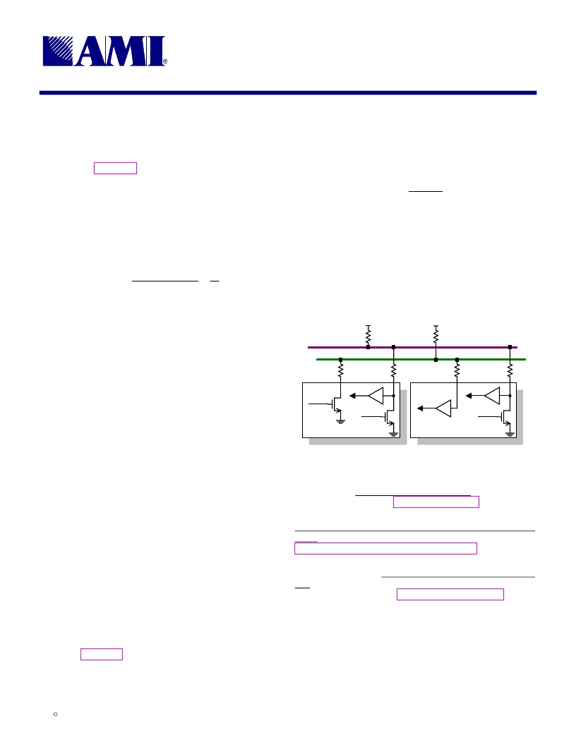
shown in Figure 20. Selection of the pull-up resistors (R
P
)
and the optional series resistors (R
S
) on the SDA and
SCL lines depends on the supply voltage, the bus ca-
Serial Communications
pacitance, and the number of connected devices with
their associated input currents.
Control of the clock and data lines is done through open
drain/collector current-sink outputs, and thus requires
external pull-up resistors on both lines. A guideline is
bus
r
P
C
t
R
×
<
2
,
where t
r
is the maximum rise time (minus some margin)
and C
bus
is the total bus capacitance. Assuming an I
2
C
device on each DIMM, an I
C controller, the clock buffer,
and two other bus devices results in values in the 5k
to
7k
range. Use of a series resistor to provide protection
against high voltage spikes on the bus will alter the val-
ues for R
P
.
Figure 20: Connections to the Serial Bus
R
P
SDA
SCL
Data In
Data Out
Clock Out
TRANSMITTER
Data In
Data Out
RECEIVER
Clock In
R
P
R
S
(optional)
R
S
(optional)
R
S
(optional)
R
S
(optional)
8.3.1
More detailed information on serial bus design can be
obtained from SMBus and I
2
C Bus Design
,
available from
the Intel Corporation at
Information on the I2
C-bus can be found in the document
The I
2
C-bus And How To Use It (Including Specifica-
tions),
available
from
Philips
http://www-us2.semiconductors.philips.com.
Additional information on the System Management Bus
can be found in the System Management Bus Specifica-
tion,
available
from
the
Implementers’ Forum at
http://www.sbs-forum.org.
For More Information
Semiconductors
at
Smart
Battery
System
相關(guān)PDF資料 |
PDF描述 |
|---|---|
| FS6053 | LOW-SKEW CLOCK FANOUT BUFFER ICs |
| FS6054 | LOW-SKEW CLOCK FANOUT BUFFER ICs |
| FS6131-01 | Programmable Line Lock Clock Generator IC |
| FS6282 | DUAL PLL CLOCK GENERATOR IC |
| FS6282-03 | DUAL PLL CLOCK GENERATOR IC |
相關(guān)代理商/技術(shù)參數(shù) |
參數(shù)描述 |
|---|---|
| FS6053 | 制造商:未知廠家 制造商全稱:未知廠家 功能描述:LOW-SKEW CLOCK FANOUT BUFFER ICs |
| FS6054 | 制造商:未知廠家 制造商全稱:未知廠家 功能描述:LOW-SKEW CLOCK FANOUT BUFFER ICs |
| FS605NA | 制造商:NETGEAR 功能描述:FS605NA FAST ENET SWITCH 制造商:NETGEAR 功能描述:NETGEAR FS605 - Switch - 5 x 10/100 - desktop |
| FS6070-01 | 制造商:未知廠家 制造商全稱:未知廠家 功能描述:Buffer/Driver |
| FS608NA | 制造商:TECH DATA 功能描述:NETGEAR FS608 - Switch - 8 x 10/100 - desktop |
發(fā)布緊急采購,3分鐘左右您將得到回復(fù)。