- 您現(xiàn)在的位置:買賣IC網(wǎng) > PDF目錄64933 > FSAT66P5X_NL (FAIRCHILD SEMICONDUCTOR CORP) 1-CHANNEL, SGL POLE SGL THROW SWITCH, PDSO5 PDF資料下載
參數(shù)資料
| 型號(hào): | FSAT66P5X_NL |
| 廠商: | FAIRCHILD SEMICONDUCTOR CORP |
| 元件分類: | 多路復(fù)用及模擬開關(guān) |
| 英文描述: | 1-CHANNEL, SGL POLE SGL THROW SWITCH, PDSO5 |
| 封裝: | 1.25 MM, SC-88A, SC-70, 5 PIN |
| 文件頁數(shù): | 4/10頁 |
| 文件大?。?/td> | 218K |
| 代理商: | FSAT66P5X_NL |
3
www.fairchildsemi.com
FSA
T
66
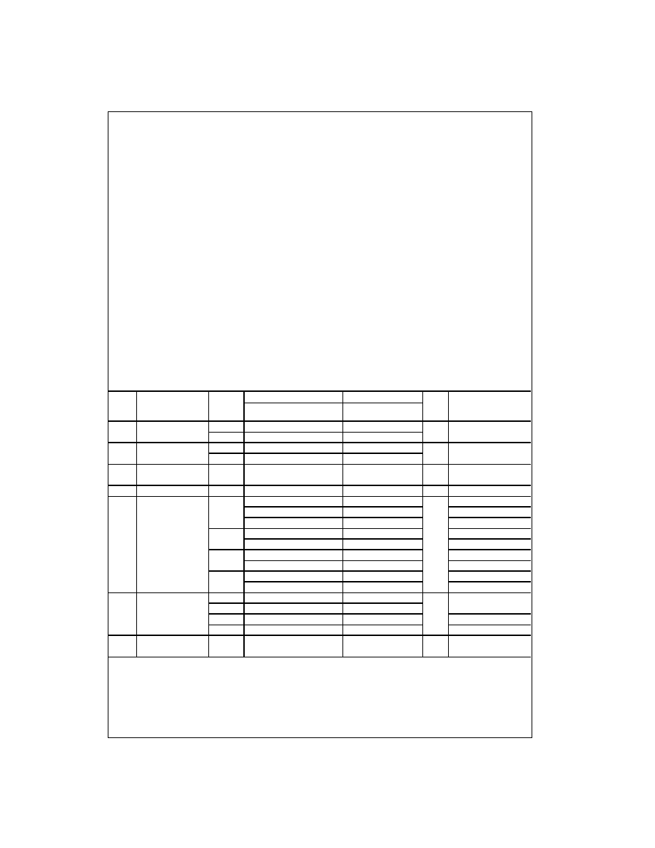
Absolute Maximum Ratings(Note 1)
Recommended Operating
Conditions (Note 3)
Note 1: The “Absolute Maximum Ratings” are those values beyond which
the safety of the device cannot be guaranteed. The device should not be
operated at these limits. The parametric values defined in the Electrical
Characteristics tables are not guaranteed at the absolute maximum ratings.
The “Recommended Operating Conditions” table will define the conditions
for actual device operation.
Note 2: The input and output negative voltage ratings may be exceeded if
the input and output diode current ratings are observed.
Note 3: Unused inputs must be held HIGH or LOW. They may not float.
DC Electrical Characteristics
Note 4: All typical values are at the specified VCC, and TA = 25°C.
Note 5: Measured by the voltage drop between A and B pins at the indicated current through the switch. On Resistance is determined by the lower of the
voltages on the two (A or B) pins.
Note 6: Parameter is characterized but not tested in production.
Note 7: Flatness is defined as the difference between the minimum and maximum value of On Resistance over the specified range of conditions.
Supply Voltage (VCC)
0.5V to +7.0V
DC Switch Voltage (VS)
0.5V to V
CC + 0.5V
DC Input Voltage (VIN) (Note 2)
0.5V to +7.0V
DC Input Diode Current
@ (IIK) VIN < 0V
50 mA
DC Output (IOUT) Sink Current
±128 mA
DC VCC or Ground Current (ICC/IGND)
±100 mA
Storage Temperature Range (TSTG)
65°C to +150°C
Junction Lead Temperature
under Bias (TJ)
+150°C
Junction Lead Temperature (TL)
(Soldering, 10 Seconds)
+260°C
Power Dissipation (PD) @ +85°C
SC70-5
150 mW
MicroPak-6
200 mW
Power Supply Voltage (VCC)
1.65V to 5.5V
Control Input Voltage (VIN)
0V to 5.5V
Switch Input Voltage (VIN)0V to VCC
Switch Output Voltage (VOUT)0V to VCC
Input Rise and Fall Time (tr, tf)
Control Input VCC = 2.3V to 3.6V
0 ns/V to 10 ns/V
Control Input VCC = 4.5V to 5.5V
0 ns/V to 5 ns/V
Switch I/O
0 ns/V to DC
Operating Temperature (TA)
40°C to +85°C
Thermal Resistance (
θ
JA)
SC70-5
425
°C/Watt
MicroPak-6
325
°C/Watt
Symbol
Parameter
VCC
(V)
TA= 40°C to +85°CTA = +25°C
Units
Conditions
Min
Typ
(Note 4)
Max
Min
Typ
Max
VIH
HIGH Level Input
4.5 to 5.5
2.0
V
Voltage
1.65 to 3.6 (0.25 VCC + 0.75)
VIL
LOW Level Input
4.5 to 5.5
0.8
V
Voltage
1.65 to 3.6
0.165 VCC
IIN
Control Input
0 to 5.5
±1.0
A0 ≤ V
IN ≤ 5.5V
Leakage Current
IOFF
OFF Leakage Current
1.65 to 5.5
±10.0
A0 ≤ A, B ≤ V
CC
RON
Switch On Resistance
4.5
3.0
7.0
VIN = 0V, IIN = 30 mA
(Note 5)
5.0
12.0
VIN = 2.4V, IIN = 15 mA
7.0
15.0
VIN = 4.5V, IIN = 30 mA
3.0
4.0
9.0
VIN = 0V, IIN = 24 mA
10.0
20.0
VIN = 3V, IIN = 24 mA
2.3
5.0
12.0
VIN = 0V, IIN = 8 mA
13.0
30.0
VIN = 2.3V, IIN = 8 mA
1.65
7.0
28.0
VIN = 0V, IIN = 4 mA
25.0
60.0
VIN = 1.65V, IIN = 4 mA
Rflat
On Resistance Flatness
5.0
6.0
IA = 30 mA, 0 ≤ VBn ≤ VCC
(Note 5)(Note 6)
3.3
12.0
IA = 24 mA, 0 ≤ VBn ≤ VCC
(Note 7)
2.5
28.0
IA = 8 mA, 0 ≤ VBn ≤ VCC
1.8
125
IA = 4 mA, 0 ≤ VBn ≤ VCC
ICC
Quiescent Supply
1.65 to 5.5
10.0
A
VIN = VCC or GND
Current
IOUT = 0
相關(guān)PDF資料 |
PDF描述 |
|---|---|
| FSB50250US | AC MOTOR CONTROLLER, DMA23 |
| FSB50825US | DC-DC REG PWR SUPPLY MODULE |
| FSDS020-557GG | SIP20, IC SOCKET |
| FSG-15N1A | SPECIALTY ANALOG CIRCUIT, SSS4 |
| FSH2050A | PLL FREQUENCY SYNTHESIZER, QCC16 |
相關(guān)代理商/技術(shù)參數(shù) |
參數(shù)描述 |
|---|---|
| FSAU3157 | 制造商:FAIRCHILD 制造商全稱:Fairchild Semiconductor 功能描述:Low-Voltage SPDT Analog Switch or 2:1 Multiplexer / De-multiplexer Bus Switch |
| FSAU3157P6X | 功能描述:模擬開關(guān) IC Low Voltage UHS SPDT Analog Switch RoHS:否 制造商:Texas Instruments 開關(guān)數(shù)量:2 開關(guān)配置:SPDT 開啟電阻(最大值):0.1 Ohms 切換電壓(最大): 開啟時(shí)間(最大值): 關(guān)閉時(shí)間(最大值): 工作電源電壓:2.7 V to 4.5 V 最大工作溫度:+ 85 C 安裝風(fēng)格:SMD/SMT 封裝 / 箱體:DSBGA-16 |
| FSAU3157P6X_Q | 功能描述:模擬開關(guān) IC Low Voltage UHS SPDT Analog Switch RoHS:否 制造商:Texas Instruments 開關(guān)數(shù)量:2 開關(guān)配置:SPDT 開啟電阻(最大值):0.1 Ohms 切換電壓(最大): 開啟時(shí)間(最大值): 關(guān)閉時(shí)間(最大值): 工作電源電壓:2.7 V to 4.5 V 最大工作溫度:+ 85 C 安裝風(fēng)格:SMD/SMT 封裝 / 箱體:DSBGA-16 |
| FSAV330 | 制造商:FAIRCHILD 制造商全稱:Fairchild Semiconductor 功能描述:4-Channel, 2:1 Video Switch |
| FSAV330_08 | 制造商:FAIRCHILD 制造商全稱:Fairchild Semiconductor 功能描述:4-Channel, 2:1 Video Switch |
發(fā)布緊急采購,3分鐘左右您將得到回復(fù)。