- 您現(xiàn)在的位置:買(mǎi)賣(mài)IC網(wǎng) > PDF目錄67592 > FSDM0265RN_NL (FAIRCHILD SEMICONDUCTOR CORP) 8 A SWITCHING REGULATOR, 73 kHz SWITCHING FREQ-MAX, PDIP8 PDF資料下載
參數(shù)資料
| 型號(hào): | FSDM0265RN_NL |
| 廠商: | FAIRCHILD SEMICONDUCTOR CORP |
| 元件分類(lèi): | 穩(wěn)壓器 |
| 英文描述: | 8 A SWITCHING REGULATOR, 73 kHz SWITCHING FREQ-MAX, PDIP8 |
| 封裝: | LEAD FREE, MS-001BA, DIP-8 |
| 文件頁(yè)數(shù): | 17/23頁(yè) |
| 文件大?。?/td> | 1073K |
| 代理商: | FSDM0265RN_NL |
第1頁(yè)第2頁(yè)第3頁(yè)第4頁(yè)第5頁(yè)第6頁(yè)第7頁(yè)第8頁(yè)第9頁(yè)第10頁(yè)第11頁(yè)第12頁(yè)第13頁(yè)第14頁(yè)第15頁(yè)第16頁(yè)當(dāng)前第17頁(yè)第18頁(yè)第19頁(yè)第20頁(yè)第21頁(yè)第22頁(yè)第23頁(yè)
FSDH0265RN, FSDM0265RN
3
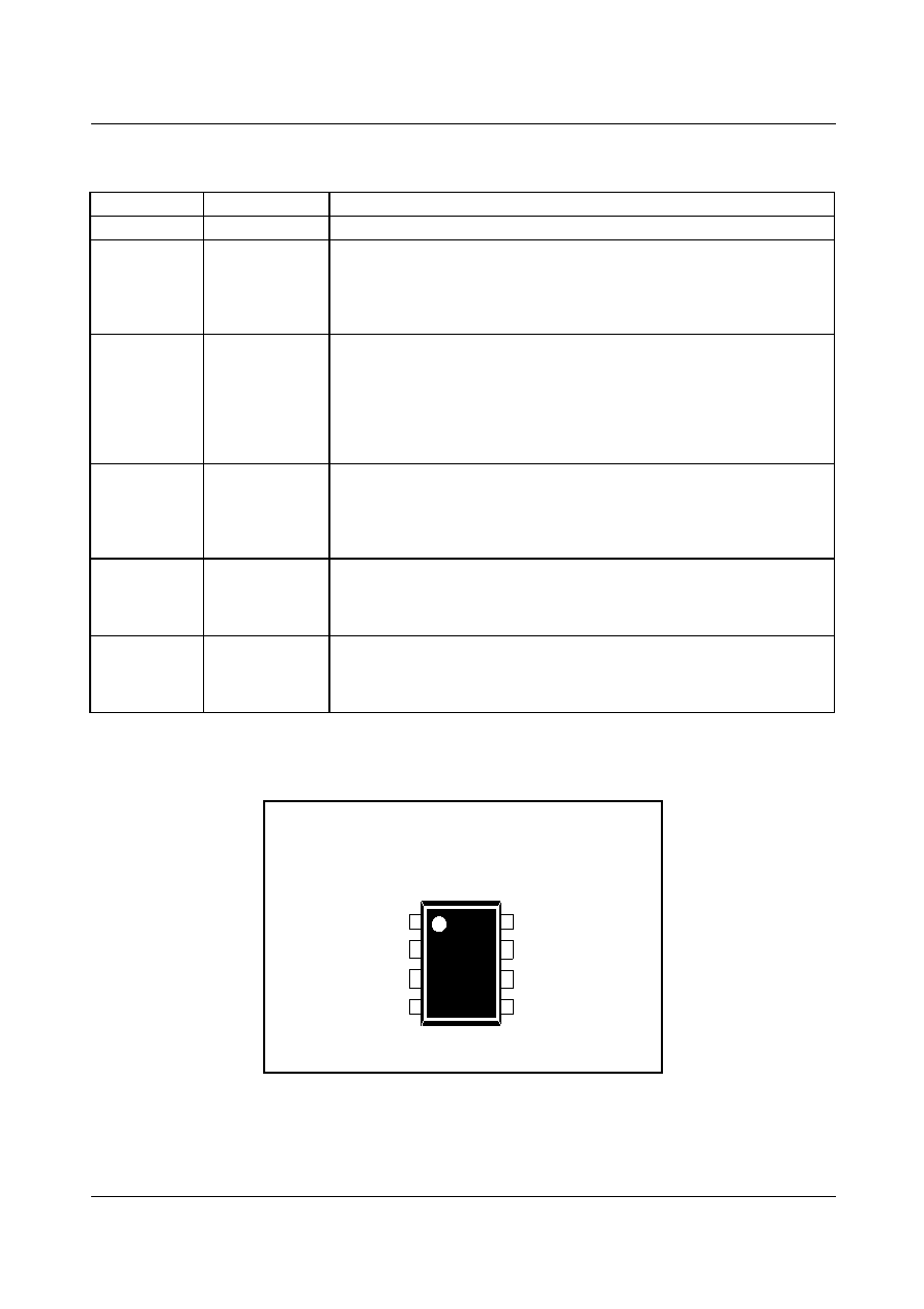
Pin Definitions
Pin Configuration
Figure 3. Pin Configuration (Top View)
Pin Number
Pin Name
Pin Function Description
1
GND
Sense FET source terminal on primary side and internal control ground.
2Vcc
Positive supply voltage input. Although connected to an auxiliary transform-
er winding, current is supplied from pin 5 (Vstr) via an internal switch during
startup (see Internal Block Diagram section). It is not until Vcc reaches the
UVLO upper threshold (12V) that the internal start-up switch opens and de-
vice power is supplied via the auxiliary transformer winding.
3Vfb
The feedback voltage pin is the non-inverting input to the PWM comparator.
It has a 0.9mA current source connected internally while a capacitor and op-
tocoupler are typically connected externally. A feedback voltage of 6V trig-
gers over load protection (OLP). There is a time delay while charging
external capacitor Cfb from 3V to 6V using an internal 5uA current source.
This time delay prevents false triggering under transient conditions, but still
allows the protection mechanism to operate under true overload conditions.
4Ipk
This pin adjusts the peak current limit of the Sense FET. The feedback
0.9mA current source is diverted to the parallel combination of an internal
2.8k
resistor and any external resistor to GND on this pin to determine the
peak current limit. If this pin is tied to Vcc or left floating, the typical peak cur-
rent limit will be 1.5A.
5Vstr
This pin connects directly to the rectified AC line voltage source. At start up
the internal switch supplies internal bias and charges an external storage
capacitor placed between the Vcc pin and ground. Once the Vcc reaches
12V, the internal switch is opened.
6, 7, 8
Drain
The drain pins are designed to connect directly to the primary lead of the
transformer and are capable of switching a maximum of 650V. Minimizing
the length of the trace connecting these pins to the transformer will decrease
leakage inductance.
1
2
3
45
6
7
8
GND
Vcc
Vfb
Ipk
Vstr
Drain
8DIP
8LSOP
相關(guān)PDF資料 |
PDF描述 |
|---|---|
| FSDH0265RL_NL | 8 A SWITCHING REGULATOR, 108 kHz SWITCHING FREQ-MAX, PDSO8 |
| FSL116LR | 1.34 A SWITCHING CONTROLLER, 54.5 kHz SWITCHING FREQ-MAX, PDIP8 |
| FSM6403MTC20X | SPECIALTY CONSUMER CIRCUIT, PDSO20 |
| FSM6403MTC | SPECIALTY CONSUMER CIRCUIT, PDSO20 |
| FSQ0765RQ | 3.92 A SWITCHING CONTROLLER, 75.8 kHz SWITCHING FREQ-MAX, ZFM6 |
相關(guān)代理商/技術(shù)參數(shù) |
參數(shù)描述 |
|---|---|
| FSDM0365RL | 功能描述:電源開(kāi)關(guān) IC - 配電 POWER_CONVERSION RoHS:否 制造商:Exar 輸出端數(shù)量:1 開(kāi)啟電阻(最大值):85 mOhms 開(kāi)啟時(shí)間(最大值):400 us 關(guān)閉時(shí)間(最大值):20 us 工作電源電壓:3.2 V to 6.5 V 電源電流(最大值): 最大工作溫度:+ 85 C 安裝風(fēng)格:SMD/SMT 封裝 / 箱體:SOT-23-5 |
| FSDM0365RLX | 功能描述:電源開(kāi)關(guān) IC - 配電 POWER_CONVERSION RoHS:否 制造商:Exar 輸出端數(shù)量:1 開(kāi)啟電阻(最大值):85 mOhms 開(kāi)啟時(shí)間(最大值):400 us 關(guān)閉時(shí)間(最大值):20 us 工作電源電壓:3.2 V to 6.5 V 電源電流(最大值): 最大工作溫度:+ 85 C 安裝風(fēng)格:SMD/SMT 封裝 / 箱體:SOT-23-5 |
| FSDM0365RN | 功能描述:電源開(kāi)關(guān) IC - 配電 POWER_CONVERSION RoHS:否 制造商:Exar 輸出端數(shù)量:1 開(kāi)啟電阻(最大值):85 mOhms 開(kāi)啟時(shí)間(最大值):400 us 關(guān)閉時(shí)間(最大值):20 us 工作電源電壓:3.2 V to 6.5 V 電源電流(最大值): 最大工作溫度:+ 85 C 安裝風(fēng)格:SMD/SMT 封裝 / 箱體:SOT-23-5 |
| FSDM0365RNB | 功能描述:電源開(kāi)關(guān) IC - 配電 SMPS Power Switch Built-in Soft Start RoHS:否 制造商:Exar 輸出端數(shù)量:1 開(kāi)啟電阻(最大值):85 mOhms 開(kāi)啟時(shí)間(最大值):400 us 關(guān)閉時(shí)間(最大值):20 us 工作電源電壓:3.2 V to 6.5 V 電源電流(最大值): 最大工作溫度:+ 85 C 安裝風(fēng)格:SMD/SMT 封裝 / 箱體:SOT-23-5 |
| FSDM0365RNC | 功能描述:開(kāi)關(guān) IC - 各種 FPS FOR DVDP/STB RoHS:否 制造商:Fairchild Semiconductor 開(kāi)啟電阻(最大值): 電源電壓-最大:4.4 V 電源電壓-最小:2.5 V 最大工作溫度:+ 85 C 最小工作溫度:- 40 C 封裝 / 箱體:WLCSP-9 封裝:Reel |
發(fā)布緊急采購(gòu),3分鐘左右您將得到回復(fù)。