- 您現(xiàn)在的位置:買賣IC網(wǎng) > PDF目錄375932 > FSDM101 (FAIRCHILD SEMICONDUCTOR CORP) Green Mode Fairchild Power Switch (FPSTM) PDF資料下載
參數(shù)資料
| 型號: | FSDM101 |
| 廠商: | FAIRCHILD SEMICONDUCTOR CORP |
| 元件分類: | 穩(wěn)壓器 |
| 英文描述: | Green Mode Fairchild Power Switch (FPSTM) |
| 中文描述: | 0.85 A SWITCHING REGULATOR, PDIP8 |
| 封裝: | MS-001BA, DIP-8 |
| 文件頁數(shù): | 10/14頁 |
| 文件大?。?/td> | 542K |
| 代理商: | FSDM101 |

FSDM101
10
Functional Description
1. Startup
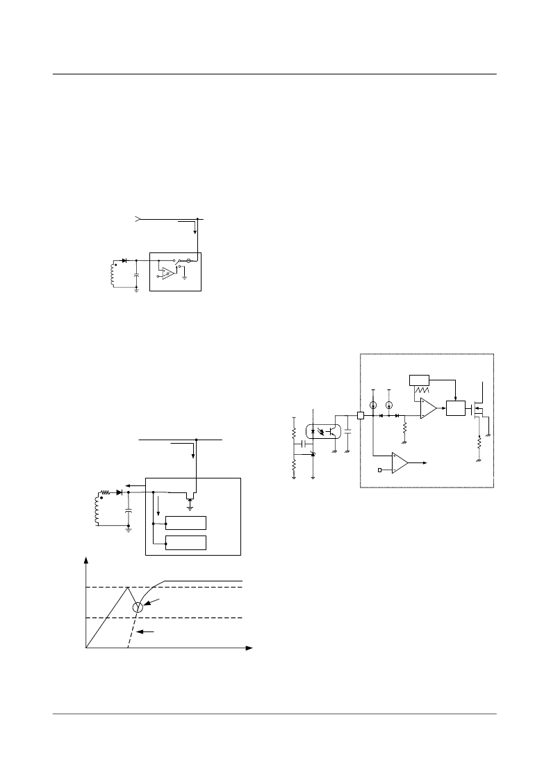
: At startup, the internal high voltage current
source supplies the internal bias and charges the external
Vcc capacitor as shown in Figure 4. In the case of the
FSDM101, when Vcc reaches 9V the device starts switching
and the internal high voltage current source is disabled. The
device continues to switch provided that Vcc does not drop
below 7V. After startup, the bias is supplied from the auxil-
iary transformer winding.
Figure 4. Internal Startup Circuit
Calculating the Vcc capacitor is an important step to design-
ing in the FSDM101. At initial start-up in the FSDM101, the
stand-by maximum current is 100uA, supplying current to
UVLO and Vref Block. The charging current (i) of the Vcc
capacitor is equal to Istr - 100uA. After Vcc reaches the
UVLO start voltage only the bias winding supplies Vcc cur-
rent to device. When the bias winding voltage is not suffi-
cient, the Vcc level decreases to the UVLO stop voltage. At
this time Vcc oscillates. In order to prevent this ripple, it is
recommended that the Vcc capacitor be sized between 10uF
and 47uF.
Figure 5. Charging the Vcc Capacitor through Vstr
2. Feedback Control
: The FSDM101 products are the volt-
age mode devices shown in Figure 6. Usually, an opto-cou-
pler and KA431 type voltage reference are used to
implement the feedback network. The feedback voltage is
compared with an internally generated sawtooth waveform.
This directly controls the duty cycle. When the KA431 refer-
ence pin voltage exceeds the internal reference voltage of
2.5V, the optocoupler LED current increases, pulling down
the feedback voltage and reducing the duty cycle. This will
happen when the input voltage increases or the output load
decreases.
3. Leading Edge Blanking (LEB)
: When the MOSFET is
turned on, there usually exists a high current spike through
the MOSFET. This is caused by primary side capacitance
and secondary side rectifier reverse recovery. This could
cause premature termination of the switching pulse if it
exceeded the over-current threshold. Therefore, the FPS
employs the leading edge blanking (LEB) circuit. This cir-
cuit inhibits the over current comparator for a short time
after the MOSFET is turned on.
Figure 6. PWM and Feedback Circuit
4. Protection Circuit
: The FSDM101 has three self protec-
tion functions: over-load protection (OLP), thermal shut-
down (TSD) and over-voltage protection (OVP). Because
these protection circuits are fully integrated into the IC with
no external components, system reliability is improved with-
out any cost increase. If either of these functions are trig-
gered, the FPS starts an auto-restart cycle. Once the fault
condition occurs, switching is terminated and the MOSFET
remains off. This causes Vcc to fall. When Vcc reaches the
UVLO stop voltage (7V), the protection is reset and the
internal high voltage current source charges the Vcc capaci-
tor. When Vcc reaches the UVLO start voltage (9V), the
device attempts to resume normal operation. If the fault con-
dition is no longer present start up will be successful. If it is,
however, still present, the cycle is repeated. This is shown in
Figure 7.
Vin,dc
Vstr
Vcc
Istr
FSDM101
9V/
7V
L
H
Vin,dc
Vstr
Istr
J-FET
UVLO
Vref
current
max
i = Istr-max current
i = Istr-max current
FSDM101
Vcc
UVLO
start
UVLO
stop
t
Vcc
Vcc must not drop
to UVLO stop
Auxiliary winding
voltage
4
OSC
Vcc
Vref
2.5uA
0.40mA
V
SD
R
FB
Gate
driver
OLP
Vfb
KA431
Cfb
Vo
相關(guān)PDF資料 |
PDF描述 |
|---|---|
| FSDM1265RBWDTU | Green Mode Fairchild Power Switch (FPS) |
| FSDM1265RB | Green Mode Fairchild Power Switch (FPS) |
| FSDM311 | Green Mode Fairchild Power Switch (FPS) |
| FSDM311L | Green Mode Fairchild Power Switch (FPS) |
| FSES0765RGWDTU | Green Mode Fairchild Power Switch (FPS) for Green Mode Fairchild Power Switch (FPSTM) for |
相關(guān)代理商/技術(shù)參數(shù) |
參數(shù)描述 |
|---|---|
| FSDM10M | 制造商:未知廠家 制造商全稱:未知廠家 功能描述:Logic IC |
| FSDM-125 | 制造商:未知廠家 制造商全稱:未知廠家 功能描述:Delay Line |
| FSDM125M | 制造商:未知廠家 制造商全稱:未知廠家 功能描述:Logic IC |
| FSDM1265RB | 制造商:FAIRCHILD 制造商全稱:Fairchild Semiconductor 功能描述:Green Mode Fairchild Power Switch (FPS) |
| FSDM1265RBWDTU | 功能描述:電源開關(guān) IC - 配電 FPS FOR LCD POWER_CONVERSION RoHS:否 制造商:Exar 輸出端數(shù)量:1 開啟電阻(最大值):85 mOhms 開啟時間(最大值):400 us 關(guān)閉時間(最大值):20 us 工作電源電壓:3.2 V to 6.5 V 電源電流(最大值): 最大工作溫度:+ 85 C 安裝風(fēng)格:SMD/SMT 封裝 / 箱體:SOT-23-5 |
發(fā)布緊急采購,3分鐘左右您將得到回復(fù)。