- 您現(xiàn)在的位置:買賣IC網(wǎng) > PDF目錄370248 > FSTD3125QSC (FAIRCHILD SEMICONDUCTOR CORP) 4-Bit Bus Switch with Level Shifting PDF資料下載
參數(shù)資料
| 型號: | FSTD3125QSC |
| 廠商: | FAIRCHILD SEMICONDUCTOR CORP |
| 元件分類: | 通用總線功能 |
| 英文描述: | 4-Bit Bus Switch with Level Shifting |
| 中文描述: | CBT/FST/QS/5C/B SERIES, QUAD 1-BIT DRIVER, TRUE OUTPUT, PDSO16 |
| 封裝: | 0.150 INCH, MO-137, QSOP-16 |
| 文件頁數(shù): | 4/7頁 |
| 文件大小: | 145K |
| 代理商: | FSTD3125QSC |
www.fairchildsemi.com
4
F
AC Electrical Characteristics
Note 6:
This parameter is guaranteed by design but is not tested. The bus switch contributes no propagation delay other than the RC delay of the typical On
Resistance of the switch and the 50pF load capacitance, when driven by an ideal voltage source (zero output impedance).
Capacitance
(Note 7)
Note 7:
T
A
=
+
25
°
C, f
=
1 MHz, Capacitance is characterized but not tested.
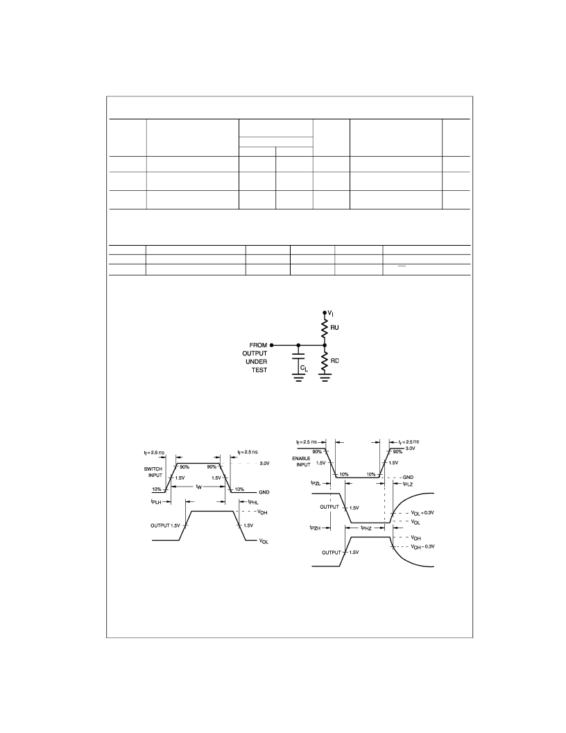
AC Loading and Waveforms
Note:
Input driven by 50
source terminated in 50
Note:
C
L
includes load and stray capacitance
Note:
Input PRR
=
1.0 MHz, t
W
=
500ns
FIGURE 1. AC Test Circuit
FIGURE 2. AC Waveforms
Symbol
Parameter
T
A
=
40
°
C to
+
85
°
C,
C
L
=
50pF, RU
=
RD
=
500
V
CC
=
4.5 – 5.5V
Min
Units
Conditions
Figure
Number
Max
0.25
t
PHL
, t
PLH
Propagation Delay Bus to Bus
(Note 6)
Output Enable Time
ns
V
I
=
OPEN
Figures
1, 2
t
PZH
, t
PZL
1.0
6.1
ns
V
I
=
7V for t
PZL
V
I
=
OPEN for t
PZH
V
I
=
7V for t
PLZ
V
I
=
OPEN for t
PHZ
Figures
1, 2
t
PHZ
, t
PLZ
Output Disable Time
1.5
6.4
ns
Figures
1, 2
Symbol
C
IN
Parameter
Typ
3
Max
Units
pF
Conditions
Control Pin Input Capacitance
V
CC
=
5.0V
C
I/O
Input/Output Capacitance
6
pF
V
CC
, OE
=
5.0V
相關(guān)PDF資料 |
PDF描述 |
|---|---|
| FSTD3125 | 4-Bit Bus Switch with Level Shifting |
| FSTD3125M | +5V, Low-Power, Parallel-Input, Voltage-Output, 12-Bit DAC |
| FSTD3125MTC | 4-Bit Bus Switch with Level Shifting |
| FSTH-03R-1 | 1.4 / 1.5 GHz Band Chip 0 deg. Splitter / Combiner |
| FSTH-03R-2 | 1.7 / 1.9 GHz Band Chip 0 deg. Splitter / Combiner |
相關(guān)代理商/技術(shù)參數(shù) |
參數(shù)描述 |
|---|---|
| FSTD3125QSCX | 功能描述:數(shù)字總線開關(guān) IC 4-Bit Bus Switch Level Shifting RoHS:否 制造商:Texas Instruments 開關(guān)數(shù)量:24 傳播延遲時間:0.25 ns 最大工作溫度:+ 85 C 最小工作溫度:- 40 C 封裝 / 箱體:TSSOP-56 封裝:Reel |
| FSTD3125Y WAF | 制造商:Fairchild Semiconductor Corporation 功能描述: |
| FSTD32211 | 制造商:FAIRCHILD 制造商全稱:Fairchild Semiconductor 功能描述:40/48-Bit Bus Switch with Level Shifting |
| FSTD32211G | 功能描述:數(shù)字總線開關(guān) IC 40/48-Bit Bus Switch RoHS:否 制造商:Texas Instruments 開關(guān)數(shù)量:24 傳播延遲時間:0.25 ns 最大工作溫度:+ 85 C 最小工作溫度:- 40 C 封裝 / 箱體:TSSOP-56 封裝:Reel |
| FSTD32211GX | 功能描述:數(shù)字總線開關(guān) IC 40/48-Bit Bus Switch Level Shifting RoHS:否 制造商:Texas Instruments 開關(guān)數(shù)量:24 傳播延遲時間:0.25 ns 最大工作溫度:+ 85 C 最小工作溫度:- 40 C 封裝 / 箱體:TSSOP-56 封裝:Reel |
發(fā)布緊急采購,3分鐘左右您將得到回復(fù)。