- 您現(xiàn)在的位置:買賣IC網(wǎng) > PDF目錄375946 > FSUSB23 (Fairchild Semiconductor Corporation) Low Power Hi-Speed USB 2.0 (480Mbps) Switch PDF資料下載
參數(shù)資料
| 型號(hào): | FSUSB23 |
| 廠商: | Fairchild Semiconductor Corporation |
| 英文描述: | Low Power Hi-Speed USB 2.0 (480Mbps) Switch |
| 中文描述: | 低功耗高速USB 2.0傳輸(480Mbps)開關(guān) |
| 文件頁(yè)數(shù): | 3/12頁(yè) |
| 文件大小: | 334K |
| 代理商: | FSUSB23 |
3
www.fairchildsemi.com
F
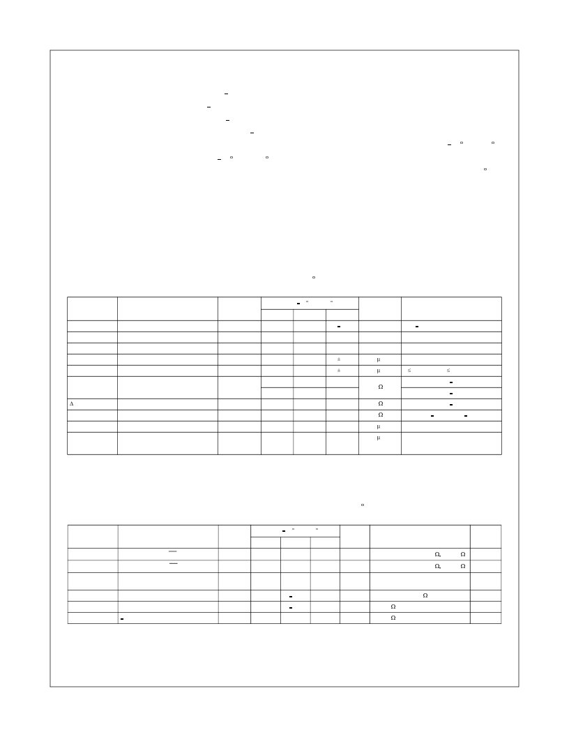
Absolute Maximum Ratings
(Note 1)
Recommended Operating Conditions
(Note 3)
Note 1:
The Absolute Maximum Ratings are those values beyond which the safety of
the device cannot be guaranteed. The device should not be operated at these limits.
The parametric values defined in the Electrical Characteristics tables are not guaran-
teed at the absolute maximum rating. The Recommended Operating Conditions
tables will define the conditions for actual device operation.
Note 2:
The input and output negative voltage ratings may be exceeded if the input
and output diode current ratings are observed. DC switch voltage may never exceed
4.6V.
Note 3:
Control input must be held HIGH or LOW and it must not float.
DC Electrical Characteristics
(All typical values are @ 25 C unless otherwise specified.)
Note 4:
Measured by the voltage drop between Dn, D1
n
, D2
n
pins at the indicated current through the switch. On Resistance is determined by the lower of the voltage on the two
ports.
Note 5:
Guaranteed by characterization.
AC Electrical Characteristics
(All typical values are for V
CC
= 3.3v @ 25 C unless otherwise specified.)
Note 6:
Guaranteed by characterization
Supply Voltage (V
CC
)
DC Switch Voltage (Note 2)
0.5V to +4.6V
0.5V to V
CC
+ 0.5V
0.5v to +4.6V
DC Input Voltage (V
IN
) (Note 2)
DC Input Diode Current
50mA
DC Output Current
50mA
Storage Temperature
65 C to +150 C
ESD (Human Body Model)
All Pins
7 KV
I/O to GND
7 KV
Supply Voltage V
CC
Control Input Voltage
3.0V to 3.6V
0V to V
CC
0V to V
CC
40 C to +85 C
Switch Input Voltage
Operating Temperature
Thermal Resistance
10 MicroPak
250 C/w
Symbol
Parameter
V
CC
T
A
= 40 C to +85 C
Units
Conditions
(V)
Min
Typ
Max
V
IK
Clamp Diode Voltage
3.0
1.2
V
I
IN
= 18mA
V
IH
Input Voltage HIGH
3.0 to 3.6
1.2
V
V
IL
Input Voltage LOW
3.0 to 3.6
0.50
V
I
IN
Control Input Leakage
3.6
1.0
A
V
IN
= 0V to V
CC
I
OZ
OFF State Leakage
1.0
A
0 Dn, D1
n
, D2
n
V
CC
R
ON
Switch On Resistance
3.0
6.0
9.0
V
IN
= 0.4V, I
ON
= 8mA
(Note 4)
7.0
10.0
V
IN
= 0.8V, I
ON
= 8mA
R
ON
Delta R
ON
(Note 5)
3.0
0.3
V
IN
= 0.8V, I
ON
= 8mA
R
ON
Flatness
R
ON
Flatness (Note 4)
3.0
2.0
V
IN
= 0.0V 1.0V, I
ON
= 8mA
I
CC
Quiescent Supply Current
3.6
1.0
A
V
IN
= 0.0V or V
CC
, I
OUT
= 0
I
CCT
Increase in I
CC
Current per
3.6
10.0
A
V
IN
= 2.6V
Control Voltage and V
CC
Levels
V
CC
= 3.6V
Symbol
Parameter
V
CC
T
A
= 40 C to +85 C
Units
Conditions
Figure
(V)
Min
Typ
Max
Number
t
ON
Turn On Time
S, OE to Output
3.0 to 3.6
10.0
13.0
ns
V
D1n
,
D2n
= 0.8V, R
L
= 50
C
L
= 10
Figure 5
t
OFF
Turn OFF Time S, OE to Output
3.0 to 3.6
8.0
11.0
ns
V
D1n
,
D2n
= 0.8V, R
L
= 50
C
L
= 10
Figure 5
t
PD
Propagation Delay (Note 6)
3.3
0.25
ns
C
L
= 10 pF
Figures 3,
4
O
IRR
OFF Isolation (Non-Adjacent)
3.0 to 3.6
30.0
dB
f = 250MHz, R
L
= 50
Figure 8
Xtalk
Non-Adjacent Channel Crosstalk
3.0 to 3.6
43.0
dB
R
L
= 50 , f = 250MHz
Figure 9
BW
3dB Bandwidth
3.0 to 3.6
720
MHz
R
L
= 50
Figure 7
相關(guān)PDF資料 |
PDF描述 |
|---|---|
| FSUSB23BQX | Low Power Hi-Speed USB 2.0 (480Mbps) Switch |
| FSUSB23L10X | Low Power Hi-Speed USB 2.0 (480Mbps) Switch |
| FSX017WF | GIGATRUE 550 CAT6 PATCH 7 FT, SNAGLESS, PURPLE |
| FSYA150D | Radiation Hardened, SEGR Resistant N-Channel Power MOSFETs |
| FSYA150D1 | Radiation Hardened, SEGR Resistant N-Channel Power MOSFETs |
相關(guān)代理商/技術(shù)參數(shù) |
參數(shù)描述 |
|---|---|
| FSUSB23_06 | 制造商:FAIRCHILD 制造商全稱:Fairchild Semiconductor 功能描述:Low Power Hi-Speed USB 2.0 (480Mbps) Switch |
| FSUSB23_08 | 制造商:FAIRCHILD 制造商全稱:Fairchild Semiconductor 功能描述:High-Speed, USB2.0 (480Mbps) Switch |
| FSUSB23BQX | 功能描述:模擬開關(guān) IC SWITCHES RoHS:否 制造商:Texas Instruments 開關(guān)數(shù)量:2 開關(guān)配置:SPDT 開啟電阻(最大值):0.1 Ohms 切換電壓(最大): 開啟時(shí)間(最大值): 關(guān)閉時(shí)間(最大值): 工作電源電壓:2.7 V to 4.5 V 最大工作溫度:+ 85 C 安裝風(fēng)格:SMD/SMT 封裝 / 箱體:DSBGA-16 |
| FSUSB23L10X | 功能描述:模擬開關(guān) IC SWITCHES RoHS:否 制造商:Texas Instruments 開關(guān)數(shù)量:2 開關(guān)配置:SPDT 開啟電阻(最大值):0.1 Ohms 切換電壓(最大): 開啟時(shí)間(最大值): 關(guān)閉時(shí)間(最大值): 工作電源電壓:2.7 V to 4.5 V 最大工作溫度:+ 85 C 安裝風(fēng)格:SMD/SMT 封裝 / 箱體:DSBGA-16 |
| FSUSB23MUX | 制造商:FAIRCHILD 制造商全稱:Fairchild Semiconductor 功能描述:Low Power Hi-Speed USB 2.0 (480Mbps) Switch |
發(fā)布緊急采購(gòu),3分鐘左右您將得到回復(fù)。