- 您現(xiàn)在的位置:買賣IC網(wǎng) > PDF目錄382972 > FW262 (Sanyo Electric Co.,Ltd.) N-Channel Silicon MOSFET PDF資料下載
參數(shù)資料
| 型號(hào): | FW262 |
| 廠商: | Sanyo Electric Co.,Ltd. |
| 英文描述: | N-Channel Silicon MOSFET |
| 中文描述: | N溝道MOSFET的硅 |
| 文件頁(yè)數(shù): | 2/2頁(yè) |
| 文件大?。?/td> | 21K |
| 代理商: | FW262 |
FW262
HD 010528-2/2
Specifications of any and all SANYO products described or contained herein stipulate the performance,
characteristics, and functions of the described products in the independent state, and are not guarantees
of the performance, characteristics, and functions of the described products as mounted in the customer's
products or equipment. To verify symptoms and states that cannot be evaluated in an independent device,
the customer should always evaluate and test devices mounted in the customer's products or equipment.
SANYO Electric Co., Ltd. strives to supply high-quality high-reliability products. However, any and all
semiconductor products fail with some probability. It is possible that these probabilistic failures could
give rise to accidents or events that could endanger human lives, that could give rise to smoke or fire,
or that could cause damage to other property. When designing equipment, adopt safety measures so
that these kinds of accidents or events cannot occur. Such measures include but are not limited to protective
circuits and error prevention circuits for safe design, redundant design, and structural design.
In the event that any or all SANYO products(including technical data,services) described or
contained herein are controlled under any of applicable local export control laws and regulations,
such products must not be exported without obtaining the export license from the authorities
concerned in accordance with the above law.
No part of this publication may be reproduced or transmitted in any form or by any means, electronic or
mechanical, including photocopying and recording, or any information storage or retrieval system,
or otherwise, without the prior written permission of SANYO Electric Co., Ltd.
Any and all information described or contained herein are subject to change without notice due to
product/technology improvement, etc. When designing equipment, refer to the "Delivery Specification"
for the SANYO product that you intend to use.
Information (including circuit diagrams and circuit parameters) herein is for example only ; it is not
guaranteed for volume production. SANYO believes information herein is accurate and reliable, but
no guarantees are made or implied regarding its use or any infringements of intellectual property rights
or other rights of third parties.
This catalog provides information as of February, 2001. Specifications and information herein are subject
to change without notice.
Continued from preceding page.
Ratings
typ
2350
390
330
Parameter
Symbol
Conditions
min
max
Unit
Input Capacitance
Output Capacitance
Reverse Transfer Capacitance
Turn-ON Delay Time
Rise Time
Turn-OFF Delay Time
Fall Time
Total Gate Charge
Gate-to-Source Charge
Gate-to-Drain “Miller” Charge
Diode Forward Voltage
Ciss
Coss
Crss
td(on)
tr
td(off)
tf
Qg
Qgs
Qgd
VSD
VDS=10V, f=1MHz
VDS=10V, f=1MHz
VDS=10V, f=1MHz
See specified Test Circuit
See specified Test Circuit
See specified Test Circuit
See specified Test Circuit
VDS=10V, VGS=10V, ID=9A
VDS=10V, VGS=10V, ID=9A
VDS=10V, VGS=10V, ID=9A
IS=9A, VGS=0
pF
pF
pF
ns
ns
ns
ns
nC
nC
nC
V
25
240
215
295
72
5
7.8
0.82
1.2
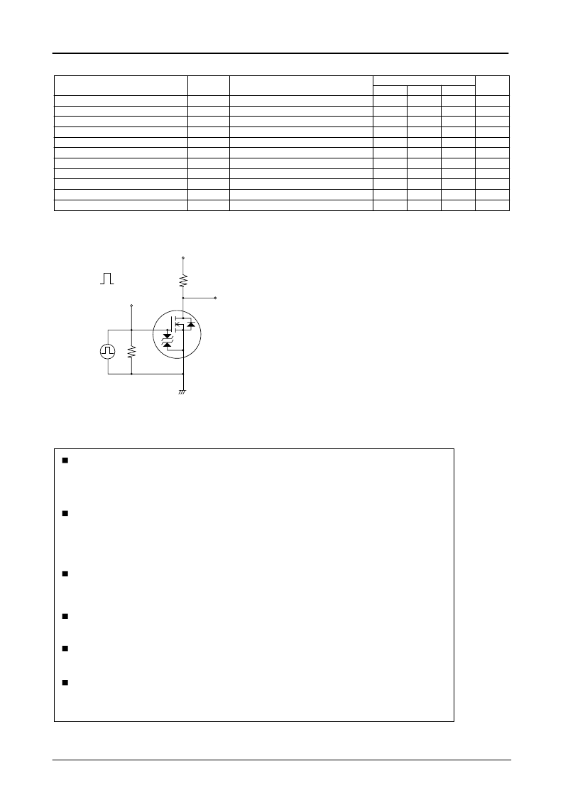
Switching Time Test Circuit
PW=10
μ
s
D.C.
≤
1%
4V
0V
VIN
P.G
50
G
S
FW262
ID= 9A
RL=1.67
VDD= 15V
VOUT
VIN
D
相關(guān)PDF資料 |
PDF描述 |
|---|---|
| FW306 | N- Channel Silicon MOS FET High Speed Switching |
| FW307 | Ultrahigh-Speed Switching Applications |
| FW30 | 30 Watt AC Adapter |
| FW3012-760-NC | 30 Watt AC Adapter |
| FW3015-760-NC | 30 Watt AC Adapter |
相關(guān)代理商/技術(shù)參數(shù) |
參數(shù)描述 |
|---|---|
| FW-27-01-F-D-220-095 | 制造商:Samtec Inc 功能描述:CONN BD STACKER HDR 54 POS 1.27MM SLDR ST TH - Bulk |
| FW-27-01-F-D-685-070 | 制造商:Samtec Inc 功能描述:CONN BD STACKER HDR 54 POS 1.27MM SLDR ST TH - Bulk |
| FW-27-01-G-D-208-130 | 制造商:Samtec Inc 功能描述:CONN BD STACKER HDR 54 POS 1.27MM SLDR ST TH - Bulk |
| FW-27-01-G-D-230-125 | 制造商:Samtec Inc 功能描述:CONN BD STACKER HDR 54 POS 1.27MM SLDR ST TH - Bulk |
| FW-27-01-G-D-661-065 | 制造商:Samtec Inc 功能描述:CONN BD STACKER HDR 54 POS 1.27MM SLDR ST TH - Bulk |
發(fā)布緊急采購(gòu),3分鐘左右您將得到回復(fù)。