- 您現(xiàn)在的位置:買賣IC網(wǎng) > PDF目錄67595 > G2996F1U (Global Mixed-mode Technology Inc.) DDR I/II Termination Regulator PDF資料下載
參數(shù)資料
| 型號: | G2996F1U |
| 廠商: | Global Mixed-mode Technology Inc. |
| 英文描述: | DDR I/II Termination Regulator |
| 中文描述: | 的DDR I / II型終端調(diào)節(jié)器 |
| 文件頁數(shù): | 12/13頁 |
| 文件大小: | 289K |
| 代理商: | G2996F1U |

Ver: 2.3
May 16, 2006
TEL: 886-3-5788833
http://www.gmt.com.tw
8
G2996
Global Mixed-mode Technology Inc.
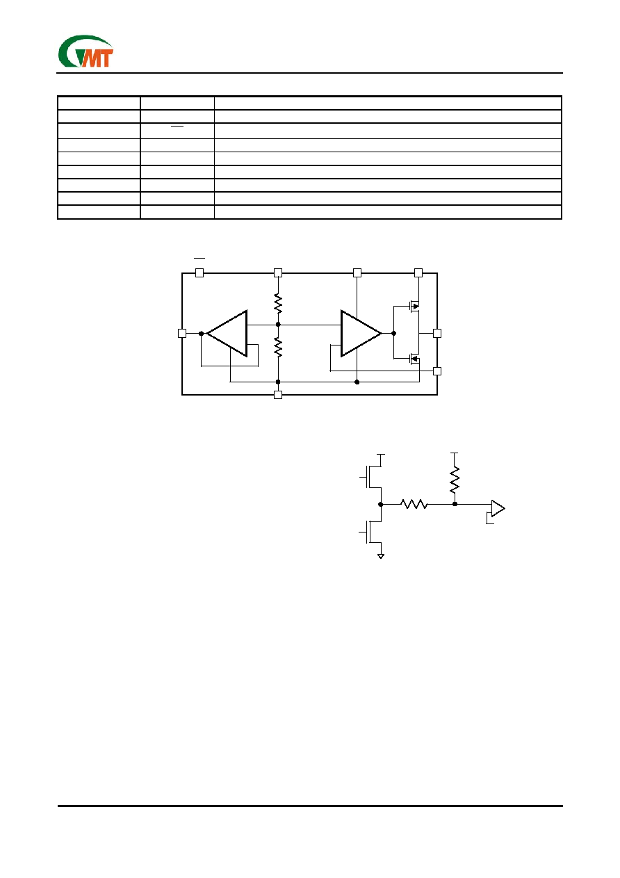
Pin Description
NUMBER
NAME
FUNCTION
1
GND
Ground
2
SD
Active low shutdown control pin
3
VSENSE
Feedback pin for regulating VTT
4
VREF
Buffered output that is a reference output of VDDQ/2
5
VDDQ
Power Input for internal reference
6
AVIN
Analog input pin
7
PVIN
Power input pin
8
VTT
Output voltage for connection to termination resistors, equal to VDDQ/2
Block Diagram
Description
The G2996 is a linear bus termination regulator de-
signed to meet the JEDEC SSTL-2 and SSTL-3 (Se-
ries Stub Termination Logic) specifications for termina-
tion of DDR-SDRAM. The output, VTT, is capable of
sinking and sourcing current while regulating the out-
put voltage equal to VDDQ/2. The G2996 is designed
to maintain the excellent load regulation and with fast
response time to minimum the transition preventing
shoot-through. The G2996 also incorporates two dis-
tinct power rails that separates the analog circuitry
(AVIN) from the power output stage (PVIN). This
power rails split can be utilized to reduce the internal
power dissipation. And this also permits G2996 to pro-
vide a termination solution for the next generation of
DDR-SDRAM (DDR II).
Series Stub Termination Logic (SSTL) was created to
improve signal integrity of the data transmission
across the memory bus. This termination scheme is
essential to prevent data error from signal reflections
while transmitting at high frequencies encountered
with DDR-SDRAM. The most common form of termi-
nation is Class II single parallel termination. This in-
volves one RS series resistor from the chipset to the
memory and one RT termination resistor, both 25
Ω
typically. The resistors can be changed to scale the
current requirements from the G2996. This implemen-
tation can be seen below in Figure 1.
AVIN, PVIN
AVIN and PVIN are two independent input supply pins
for the G2996. AVIN is used to supply all the internal
analog circuits. PVIN is only used to supply the output
stage to create the regulated VTT. To keep the regula-
tion successfully, AVIN should be equal to or larger
than PVIN. Using a higher PVIN voltage will produce a
larger sourcing capability from VTT. But the internal
power loss will also increase and then the heat in-
creases. If the junction temperature exceeds the
thermal shutdown threshold than the G2996 will enter
the shutdown state that is the same as manual shut-
down, where VTT is tri-state and VREF remains active.
For SSTL-2 applications, the AVIN and PVIN can be
short together at 2.5V to minimize the PCB complexity
and to reduce the bypassing capacitors for the two
supply pins separately.
+
-
+
-
PV
IN
AV
IN
V
DDQ
SD
50k
GND
V
REF
V
SENSE
V
TT
+
-
+
-
+
-
+
-
PV
IN
AV
IN
V
DDQ
SD
50k
GND
V
REF
V
SENSE
V
TT
V
DD
CHIPSET
R
S
V
TT
R
T
MENORY
V
REF
Figure 1. SSTL-Termination Scheme
V
DD
CHIPSET
R
S
V
TT
R
T
MENORY
V
REF
Figure 1. SSTL-Termination Scheme
相關(guān)PDF資料 |
PDF描述 |
|---|---|
| G2996P1UF | DDR I/II Termination Regulator |
| G2996P1U | DDR I/II Termination Regulator |
| G5105TBU | Low-Noise Step-up DC-DC Converter |
| G5105TPU | Low-Noise Step-up DC-DC Converter |
| G5105 | Low-Noise Step-up DC-DC Converter |
相關(guān)代理商/技術(shù)參數(shù) |
參數(shù)描述 |
|---|---|
| G2996F1UF | 制造商:GMT 制造商全稱:Global Mixed-mode Technology Inc 功能描述:DDR I/II Termination Regulator |
| G2996P1U | 制造商:GMT 制造商全稱:Global Mixed-mode Technology Inc 功能描述:DDR I/II Termination Regulator |
| G2996P1UF | 制造商:GMT 制造商全稱:Global Mixed-mode Technology Inc 功能描述:DDR I/II Termination Regulator |
| G2997 | 制造商:GMT 制造商全稱:Global Mixed-mode Technology Inc 功能描述:DDR Termination Regulator |
| G2997B | 制造商:GMT 制造商全稱:Global Mixed-mode Technology Inc 功能描述:DDR Termination Regulator |
發(fā)布緊急采購,3分鐘左右您將得到回復(fù)。