- 您現(xiàn)在的位置:買賣IC網(wǎng) > PDF目錄60264 > G525A2 (Global Mixed-mode Technology Inc.) USB High-Side Power Switch Advance Information PDF資料下載
參數(shù)資料
| 型號: | G525A2 |
| 廠商: | Global Mixed-mode Technology Inc. |
| 英文描述: | USB High-Side Power Switch Advance Information |
| 中文描述: | 的USB高側(cè)電源開關(guān)進展信息 |
| 文件頁數(shù): | 5/8頁 |
| 文件大小: | 243K |
| 代理商: | G525A2 |
Ver: 1.2
Nov 11, 2002
TEL: 886-3-5788833
http://www.gmt.com.tw
5
G525A
Global Mixed-mode Technology Inc.
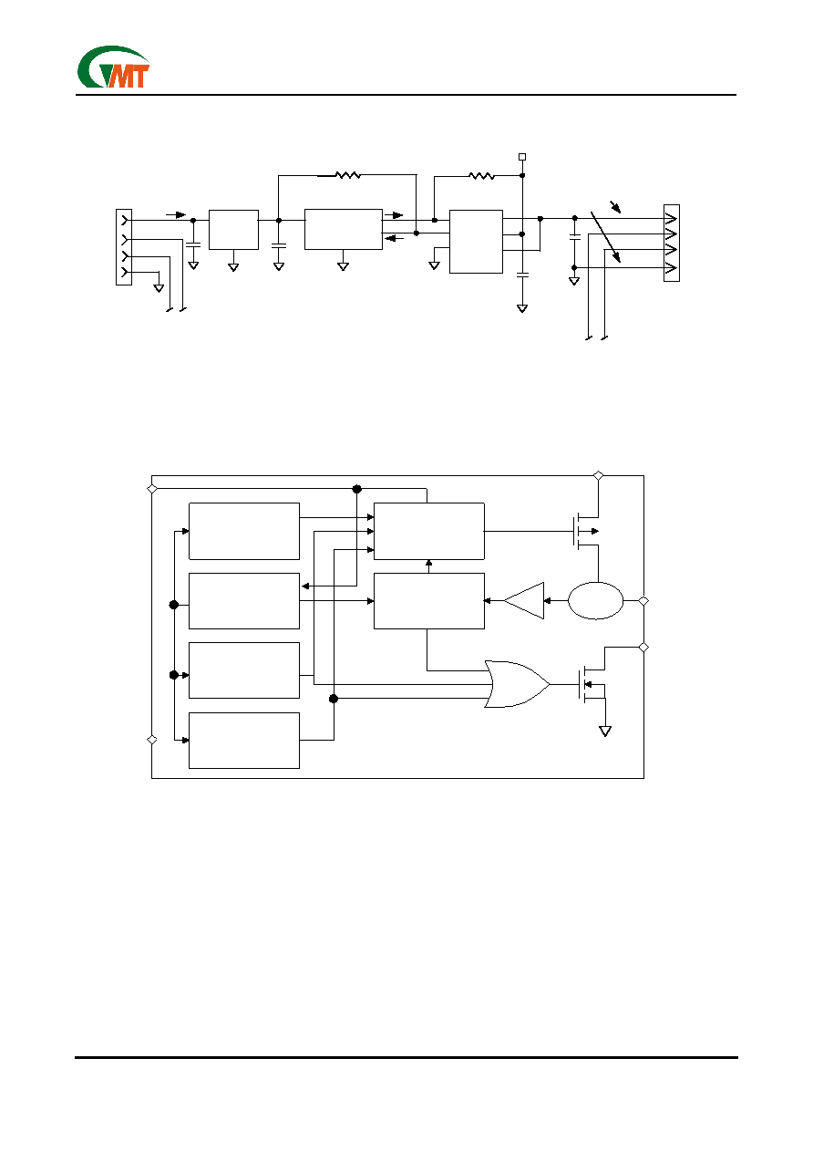
Typical Applications
Single-Port Self-Powered USB Hub Application
Function Block Diagrams
Functional Description
The G525A1 and G525A2 are high-side 1-channel
switches with active-high and active-low enable inputs,
respectively. Fault conditions turn off or inhibit turn-on
of the output transistors and activate the open-drain
error flag transistors to pull FLG pin to ground.
Input and Output
IN (input) is the power supply connection to the logic
circuitry and the source of the output MOSFET. OUT
(output) is the drain of the output MOSFET. In a typical
application, current flows through the switch from IN to
OUT toward the load. Both OUT pins must be
connected together to the load.
The output MOSFET and driving circuit are also de-
signed to allow the MOSFET drain to be externally
forced to a higher voltage than the source (VOUT > VIN)
when the switch is off. In this situation, the G525A
avoids undesirable drain-to-body diode current flow by
connecting the body to the most positive voltage. If
VOUT >VIN when switch is enabled, current will flow
from VOUT to VIN.
Thermal Shutdown
Thermal shutdown protects G525A from excessive
power dissipation. If the die temperature exceeds
135°C, the MOSFETS switch is shut off and a fault
flag is activated. 10°C of hystersis prevents the switch
Upstream
V
BUS
100mA max.
V
CC
5.0V
V
BUS
D
+
D
-
GND
Data
GND
IN
OUT
3.3V USB Controller
VIN
ON/OFF
OVERCURRENT
G525A
EN
OUT
FLG
IN
GND OUT
+
USB
Port
Data
V
BUS
D
+
D
-
GND
Ferrite
Beads
10k
100k
1F
NC
GND
0.1 F
150 F
1 F
NC
G912
Upstream
V
BUS
100mA max.
V
CC
5.0V
V
BUS
D
+
D
-
GND
Data
GND
IN
OUT
3.3V USB Controller
VIN
ON/OFF
OVERCURRENT
G525A
EN
OUT
FLG
IN
GND OUT
+
USB
Port
Data
V
BUS
D
+
D
-
GND
Ferrite
Beads
10k
100k
1F
NC
GND
0.1 F
150 F
1 F
NC
G912
Clock
BandGap
Reference
UVLO
Thermal Sense
Overcurrent
Limiting
Gate Control
Current
Sense
CMP
IN
OUT
FLG
EN
GND
Clock
BandGap
Reference
UVLO
Thermal Sense
Overcurrent
Limiting
Gate Control
Current
Sense
CMP
IN
OUT
FLG
EN
GND
相關(guān)PDF資料 |
PDF描述 |
|---|---|
| G528A | USB High-Side Power Switch Advance Information |
| G528AP1U | USB High-Side Power Switch Advance Information |
| G528AP1UF | USB High-Side Power Switch Advance Information |
| G528P1U | USB High-Side Power Switch Advance Information |
| G528P1UF | USB High-Side Power Switch Advance Information |
相關(guān)代理商/技術(shù)參數(shù) |
參數(shù)描述 |
|---|---|
| G526 | 制造商:未知廠家 制造商全稱:未知廠家 功能描述:Dual USB High-Side Power Switch |
| G526-1 | 制造商:未知廠家 制造商全稱:未知廠家 功能描述:Dual USB High-Side Power Switch |
| G526-2 | 制造商:未知廠家 制造商全稱:未知廠家 功能描述:Dual USB High-Side Power Switch |
| G528 | 制造商:GMT 制造商全稱:Global Mixed-mode Technology Inc 功能描述:USB High-Side Power Switch Advance Information |
| G52803014AEU | 制造商:Amphenol Corporation 功能描述: |
發(fā)布緊急采購,3分鐘左右您將得到回復。