- 您現(xiàn)在的位置:買(mǎi)賣(mài)IC網(wǎng) > PDF目錄60264 > G525A (Global Mixed-mode Technology Inc.) USB High-Side Power Switch Advance Information PDF資料下載
參數(shù)資料
| 型號(hào): | G525A |
| 廠商: | Global Mixed-mode Technology Inc. |
| 英文描述: | USB High-Side Power Switch Advance Information |
| 中文描述: | 的USB高側(cè)電源開(kāi)關(guān)進(jìn)展信息 |
| 文件頁(yè)數(shù): | 2/8頁(yè) |
| 文件大小: | 243K |
| 代理商: | G525A |
Ver: 1.2
Nov 11, 2002
TEL: 886-3-5788833
http://www.gmt.com.tw
2
G525A
Global Mixed-mode Technology Inc.
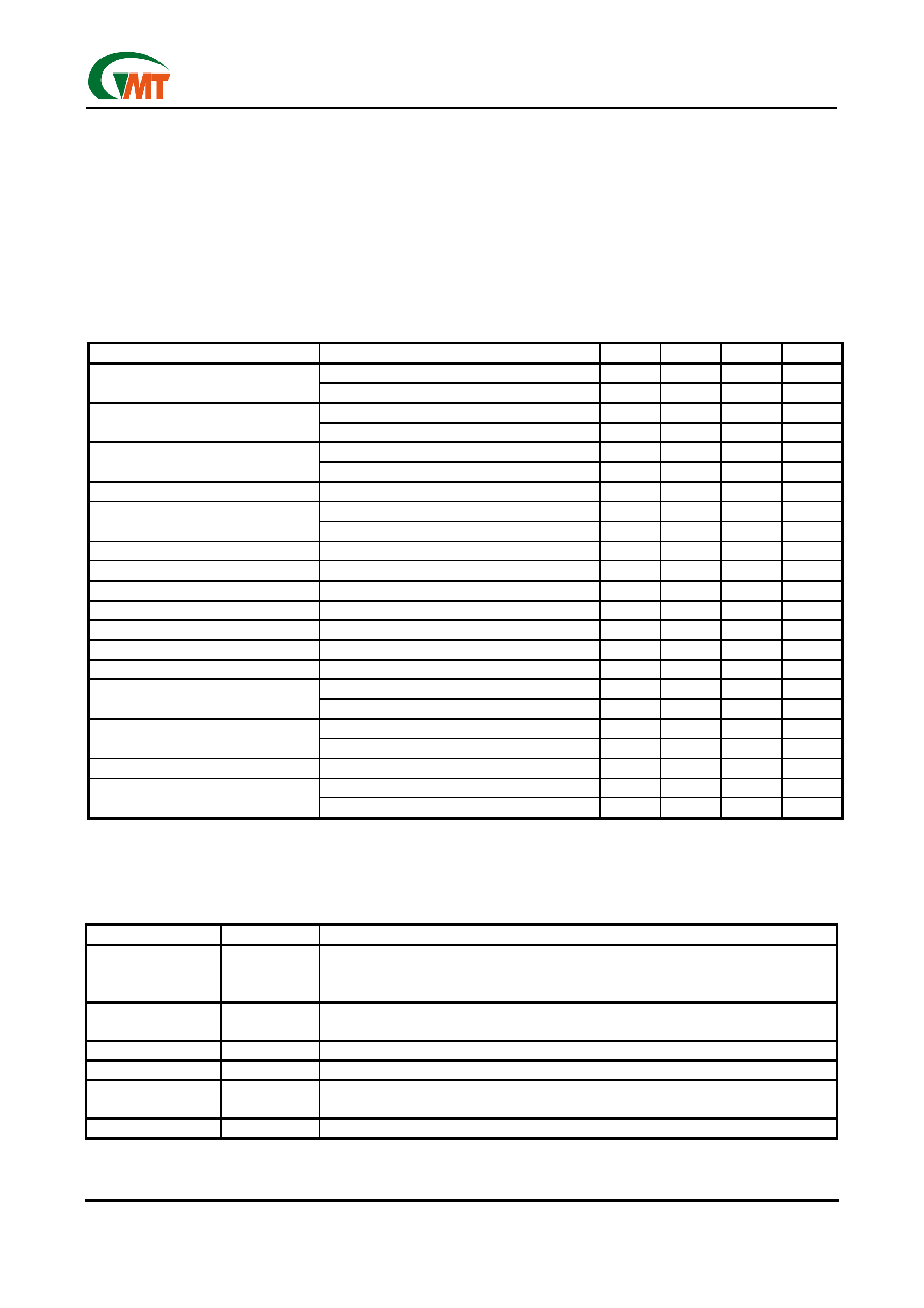
Absolute Maximum Ratings
Supply Voltage (VIN)..…………….….………...…..+6.0V
Fault Flag Voltage (VFLG)..…………..……...……..+6.0V
Fault Flag Current (IFLG)……………………………50mA
Output Voltage (VOUT)..…………………………….+6.0V
Output Current (IOUT).………………….Internally Limited
Enable Input (VEN)……………………………-0.3V to 6V
Storage Temperature (TS)….………....-65°C to +150°C
Lead Temperature (Soldering 5 sec.)……………260°C
ESD protection*………………..…………….……….2kV
Operating Ratings
Supply Voltage (VIN).……………………….+3V to +5.5V
Operating Temperature (TA)…………….-40°C to +85°C
Thermal Resistance
SOIC (θJA)……………………………………160°C/W
Electrical Characteristics (V
IN=+5V; TA=25°C.)
PARAMETER
CONDITION
MIN
TYP
MAX
UNITS
**switch off, OUT = open
1
5
A
IN Supply Current
**switch on, OUT = open
100
160
A
low to high transition
2.5
V
EN Enable Threshold
high to low transition **
0.8
V
VEN = VOH(min) = 2.5V
0.01
1
A
EN Input Current
VEN = VOL(max) = 1.0V
0.01
1
A
EN Input Capacitance
1
pF
VIN = 5V , IOUT = 500mA
110
140
m
Switch Resistance
VIN = 3.3V , IOUT = 500mA
130
180
m
OUT Turn-On Delay
RL = 10
0.03
ms
OUT Turn-On Rise Time
RL = 10
, CL=100F
0.5
ms
OUT Turn-Off Delay
RL = 10
1
20
s
OUT Turn-Off Fall Time
RL = 10
1
20
s
OUT Leakage Current
1
10
A
Short Circuit Current Limit
Enable into load
1.0
1.4
2.0
A
Circuit Limit Threshold
Ramped load applied to enabled output
2.0
2.7
3.5
A
TJ increasing
135
°C
Overtemperature Shutdown
Threshold
TJ decreasing
125
°C
VIN = 5V, IL=10mA
10
25
Ω
FLG Output Resistance
VIN = 3.3V, IL =10mA
15
40
Ω
FLG Off Current
VFLAG = 5V
0.01
1
A
VIN = increasing
2.5
V
UVLO Threshold
VIN = decreasing
2.3
V
* Devices are ESD protected, however, handling precautions are recommended.
** For the G525A1, off is
≤ 1.0 and on is ≥2.5V. For the G525A2, off is ≥ 2.5V and on is ≤ 1.0V. The enable input,
CTRL, has approximately 200mV of hysteresis.
Pin Description
PIN NUMBER
PIN NAME
PIN FUNCTION
1
EN
Enable (input): Logic level enable input. High input >2.4V typical.
Low input <2.2V typical (1 for active high, 2 for active low).
Make sure EN never floating.
2
FLG
Open-Drain Fault Flag (Output): Active-low, open-drain output. Indicates overcurrent,
thermal shutdown and UVLO.
3
GND
Ground.
4,5
NC
Not internally connected.
7
IN
Input Supply: Output MOSFET source, which also supplies IC's internal circuitry. Con-
nect to positive supply.
6,8
OUT
Switch Output: Output MOSFET drain. Typically connect to switched side of load.
相關(guān)PDF資料 |
PDF描述 |
|---|---|
| G525A1 | USB High-Side Power Switch Advance Information |
| G525A2 | USB High-Side Power Switch Advance Information |
| G528A | USB High-Side Power Switch Advance Information |
| G528AP1U | USB High-Side Power Switch Advance Information |
| G528AP1UF | USB High-Side Power Switch Advance Information |
相關(guān)代理商/技術(shù)參數(shù) |
參數(shù)描述 |
|---|---|
| G525A1 | 制造商:GMT 制造商全稱:Global Mixed-mode Technology Inc 功能描述:USB High-Side Power Switch Advance Information |
| G525A2 | 制造商:GMT 制造商全稱:Global Mixed-mode Technology Inc 功能描述:USB High-Side Power Switch Advance Information |
| G526 | 制造商:未知廠家 制造商全稱:未知廠家 功能描述:Dual USB High-Side Power Switch |
| G526-1 | 制造商:未知廠家 制造商全稱:未知廠家 功能描述:Dual USB High-Side Power Switch |
| G526-2 | 制造商:未知廠家 制造商全稱:未知廠家 功能描述:Dual USB High-Side Power Switch |
發(fā)布緊急采購(gòu),3分鐘左右您將得到回復(fù)。