- 您現(xiàn)在的位置:買賣IC網(wǎng) > PDF目錄67595 > G574SAF (Global Mixed-mode Technology Inc.) Dual-Slot PCMCIA/CardBus Power Controller PDF資料下載
參數(shù)資料
| 型號(hào): | G574SAF |
| 廠商: | Global Mixed-mode Technology Inc. |
| 英文描述: | Dual-Slot PCMCIA/CardBus Power Controller |
| 中文描述: | 雙插槽的PCMCIA / CardBus電源控制器 |
| 文件頁數(shù): | 9/16頁 |
| 文件大小: | 367K |
| 代理商: | G574SAF |
Ver: 1.2
Jul 28, 2006
TEL: 886-3-5788833
http://www.gmt.com.tw
2
G574
Global Mixed-mode Technology Inc.
Absolute maximum ratings over operating
free-air temperature (unless otherwise noted)*
Input voltage range for card power:
VI(3.3V) . . . . . . . . . . . . . . . . . . . . . . . . . . . . . -0.3V to 6V
VI(5V) . . . . . . . . . . . . . . . . . . . . . . . . . . . . . . -0.3V to 6V
VI(12V) . . . . . . . . . . . . . . . . . . . . . . . . . . . . .-0.3V to 14V
Logic input voltage. . . . . . . . . . . . . . . . . . . -0.3V to 6V
Output current (each card):
IO (xVCC) . . . . . . . . . . . . . . . . . . . . . . . . internally limited
IO(xVPP) . . . . . . . . . . . . . . . . . . . . . . . . .internally limited
Operating virtual junction temperature range, TJ
. . . . . . . . . . . . . . . . . . . . . . . . . . . . . . . -40°C to 125°C
Operating free-air temperature range, TA
. . . . . . . . . . . . . . . .. . . . . . . . . . . . . . . . .-40°C to 85°C
Storage temperature range,
TSTG. . . . . . . . . . . . . . . . . . . . . . . . . . . .-55°C to 150°C
Thermal resistance
θ
JA
SSOP-30. . . . . . . . . . . . . . . . . . . . . . . . . . . . .122°C/W
Power dissipation PD (TA ≤ +25°C)
SSOP-30. . . . . . . . . . . . . . . . . . . . . . . . . . . . .1024mW
ESD. . . . . . . . . . . . . . . . .. . . . . . . . . . . . . . . . . . .Note1
*Stresses beyond those listed under “absolute maximum ratings” may cause permanent damage to the device. These are stress rating
only, and functional operation of the device at these or any other conditions beyond those indicated under “recommended operating
conditions” is not implied. Exposure to absolute-maximum-rated conditions for extended periods may affect device reliability.
Note 1: ESD (electrostatic discharge) sensitive device. Proper ESD precautions are recommended to avoid performance degradation or
less of functionality.
Recommended Operating Conditions
Min
Max
Unit
VI (5V)
2.7
5.25
V
VI (3.3V)
2.7
5.25
V
Input voltage range, VI
VI (12V)
---
13.5
V
IO (xVCC) at 25°C
---
1
A
Output current
IO (xVPP) at 25°C
---
150
mA
Clock frequency
0
2.5
MHz
Operating virtual junction temperature, TJ
-40
125
°C
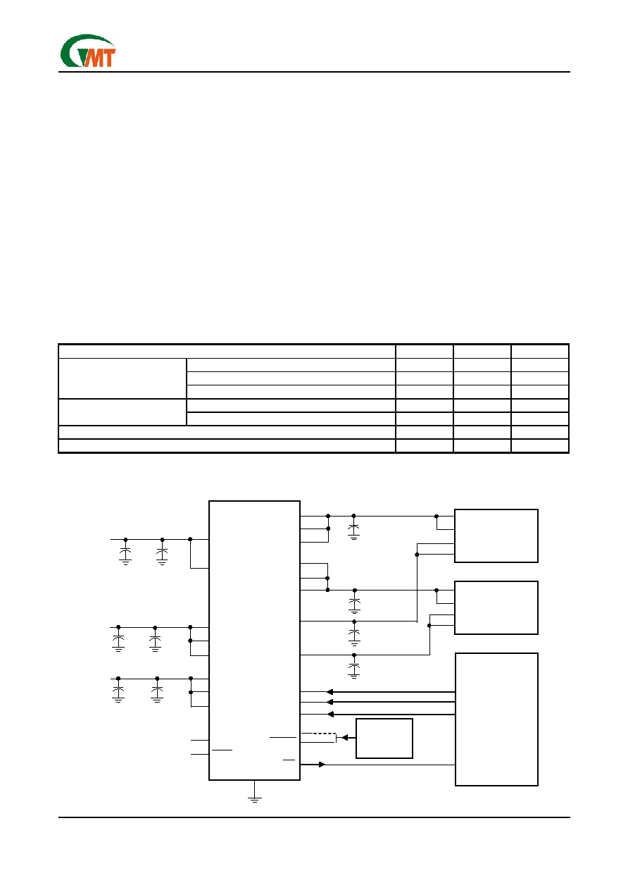
Typical PC Card Power-Distribution Application
0.1F
12V
AVCC
BVCC
AVPP
BVPP
DATA
CLOCK
LATCH
RESET
OC
System Voltage
Supervisor
or
PCI Bus Reset
0.1F
V
CC
V
CC
PC Card
Connector A
V
PP1
V
PP2
PC Card
Connector B
V
PP2
V
PP1
V
CC
V
CC
DATA
CLOCK
LATCH
PCMCIA
Controller
5V
3.3V
33F
0.1F
33F
0.1F
5V
3.3V
GND
G574
0.1F
10F
12V
(Ceramic)
STBY
MODE
GPI/O
0.1F
12V
AVCC
BVCC
AVPP
BVPP
DATA
CLOCK
LATCH
RESET
OC
System Voltage
Supervisor
or
PCI Bus Reset
0.1F
V
CC
V
CC
PC Card
Connector A
V
PP1
V
PP2
PC Card
Connector B
V
PP2
V
PP1
V
CC
V
CC
DATA
CLOCK
LATCH
PCMCIA
Controller
5V
3.3V
33F
0.1F
33F
0.1F
5V
3.3V
GND
G574
0.1F
10F
12V
(Ceramic)
STBY
MODE
GPI/O
相關(guān)PDF資料 |
PDF描述 |
|---|---|
| G574SA | Dual-Slot PCMCIA/CardBus Power Controller |
| G576 | CAP TAN CHIP 100.0UF10.00% 16.0V 85C 2918 LOWESR |
| G670 | Microprocessor Reset IC |
| G671L438T25UF | Microprocessor Reset IC |
| G671L438T25U | Microprocessor Reset IC |
相關(guān)代理商/技術(shù)參數(shù) |
參數(shù)描述 |
|---|---|
| G575003S | 制造商:GRAND-TEK TECHNOLOGY 功能描述:50W CBL MNT PLG |
| G575215A | 制造商:ITT Interconnect Solutions 功能描述:Air driven diaphragm pump, 28 lpm |
| G575A10 | 制造商:Crouzet 功能描述:Relay SSR 10mA 280V AC-IN 10A 660V AC-OUT 4-Pin |
| G575A25 | 制造商:Crydom 功能描述: |
| G575A50 | 制造商:Crouzet 功能描述:Relay SSR 10mA 280V AC-IN 50A 660V AC-OUT 4-Pin |
發(fā)布緊急采購,3分鐘左右您將得到回復(fù)。