- 您現(xiàn)在的位置:買賣IC網(wǎng) > PDF目錄382995 > GB4570-CKA (Electronic Theatre Controls, Inc.) Monolithic Video Buffer/Clamp PDF資料下載
參數(shù)資料
| 型號: | GB4570-CKA |
| 廠商: | Electronic Theatre Controls, Inc. |
| 英文描述: | Monolithic Video Buffer/Clamp |
| 中文描述: | 單片視頻緩沖器/鉗 |
| 文件頁數(shù): | 3/5頁 |
| 文件大?。?/td> | 149K |
| 代理商: | GB4570-CKA |
3
521 - 18 - 01
With this automatic adjustment system, the need for an external
sync separator circuit to enable the clamping action is
eliminated.
The input to the GB4570 must be AC coupled using an
appropriately sized capacitor. This capacitor acts as a DC
reservoir for corrective level shifts. Under equilibrium
conditions, the average current supplied by the comparator
output is just sufficient to balance the current discharging the
input coupling capacitor. Under dynamic conditions, where
the system is correcting for a change in the signal level, the
charging current may be in the milliamp range. Since the
corrective current is small under equilibrium conditions, the
error voltage at the comparator input is also small making
clamping to within
±
2 mV achievable.
The circuit makes use of a ‘peak hold’ capacitor, C
HOLD
, at the
output of the comparator. This gives rise to a more constant
voltage at the comparator output. This constant voltage is
translated to a more constant corrective current by an internal
50 k
resistor between the comparator output and the signal
input.
To avoid excessive phase shifts and consequent instability of
the clamp feedback loop, the peak hold capacitor should be
considerably smaller (eg. 1000 times smaller) than the input
coupling capacitor. If faster clamping is desirable, the peak
hold capacitor can be removed and a smaller input coupling
capacitor employed. In this application, some distortion of the
signal tip will occur.
DETAILED DESCRIPTION
The GB4570 is intended for video applications requiring DC
restoration. The GB4570 signal path consists of a wideband
Darlington emitter follower for maximum bandwidth
performance. With this configuration, the GB4570’s small
signal frequency response remains within
±
0.1 dB of 0 dB out
to 80 MHz.
Optimal frequency response for the GB4570 occurs with load
capacitance in the range of 15 pF. For smaller loads, an
external capacitor can be added to maximize the bandwidth
of the device. As shown in Figure 1, a small resistor, R
OUT
,
should be included in series with the GB4570 output to obtain
optimal response flatness. For a nominal load of 15 pF, R
OUT
should be chosen to be approximately 40
.
The DC restoration function is achieved through the use of a
simple comparator. The non-inverting input of the comparator
is connected to the clamp reference voltage, while the inverting
input is connected to the GB4570 output. For output signals
more positive than the clamp reference voltage, the comparator
output is essentially open-circuit, while signal voltages more
negative than the clamp reference voltage result in the charging
of C
, an external non-polar capacitor connected to pin 4.
The action of the comparator is to provide a positive current
which is fed back to the input under conditions where the
device output is more negative than the clamp reference
voltage. This negative feedback raises the DC level of the
input signal to the point where all signal fluctuations occur at
voltages above the clamp reference voltage.
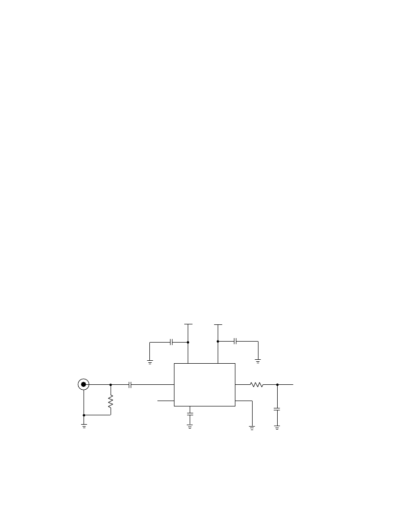
All resistors are in ohms, all capacitors in microfarads unless otherwise stated
Fig. 1 Typical Application Circuit
75
VIDEO
1.1nF
V
CC
V
EE
8 6
2
3
4 1
C
LOAD
C
HOLD
V
CLAMP
V
IN
R
OUT
CLAMPED
VIDEO
OUTPUT
22
0.1
0.1
GB4570
CLAMP
相關PDF資料 |
PDF描述 |
|---|---|
| GB4570-CTA | Monolithic Video Buffer/Clamp |
| GB4571-CTA | Video Buffer with Precision Strobed DC Restore |
| GB4571 | Video Buffer with Precision Strobed DC Restore |
| GB4571-CDA | Video Buffer with Precision Strobed DC Restore |
| GB4571-CKA | Video Buffer with Precision Strobed DC Restore |
相關代理商/技術參數(shù) |
參數(shù)描述 |
|---|---|
| GB4570-CTA | 制造商:未知廠家 制造商全稱:未知廠家 功能描述:Monolithic Video Buffer/Clamp |
| GB4571 | 制造商:GENNUM 制造商全稱:GENNUM 功能描述:Video Buffer with Precision Strobed DC Restore |
| GB4571-CDA | 制造商:GENNUM 制造商全稱:GENNUM 功能描述:Video Buffer with Precision Strobed DC Restore |
| GB4571CKA | 制造商:Gennum Corporation 功能描述: |
| GB4571-CKA | 制造商:未知廠家 制造商全稱:未知廠家 功能描述:Video Buffer with Precision Strobed DC Restore |
發(fā)布緊急采購,3分鐘左右您將得到回復。