- 您現(xiàn)在的位置:買賣IC網(wǎng) > PDF目錄375997 > GF9331 GF9331 - HDTV/SDTV Motion Co-processor PDF資料下載
參數(shù)資料
| 型號: | GF9331 |
| 英文描述: | GF9331 - HDTV/SDTV Motion Co-processor |
| 中文描述: | GF9331 -高清/標(biāo)清運(yùn)動協(xié)處理器 |
| 文件頁數(shù): | 17/34頁 |
| 文件大小: | 550K |
| 代理商: | GF9331 |
第1頁第2頁第3頁第4頁第5頁第6頁第7頁第8頁第9頁第10頁第11頁第12頁第13頁第14頁第15頁第16頁當(dāng)前第17頁第18頁第19頁第20頁第21頁第22頁第23頁第24頁第25頁第26頁第27頁第28頁第29頁第30頁第31頁第32頁第33頁第34頁

GENNUM CORPORATION
18283 - 3
17
G
5.2 Host Interface Parallel Mode
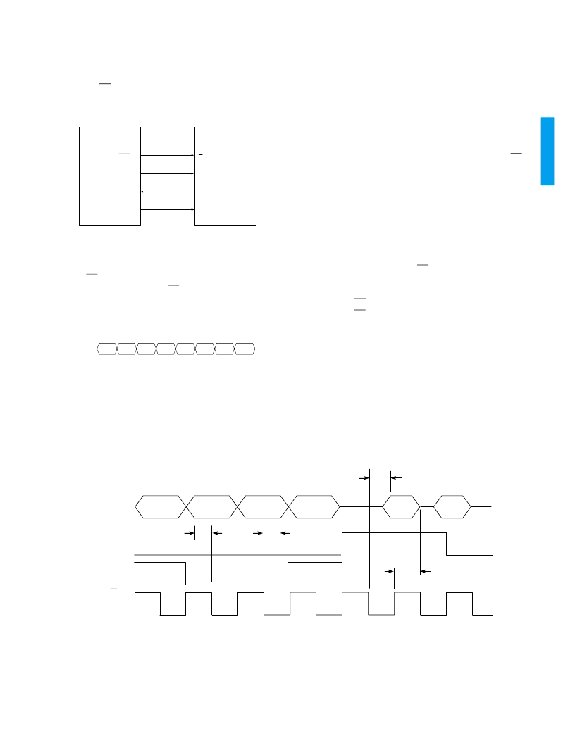
The Gennum Parallel Peripheral Interface (GPPI) consists of
an 8-bit multiplexed address/data bus (DAT_IO[7:0]), a chip
select pin (CS), a read/write pin (R_W), and an address/
data pin (A_D) as shown in Figure 9.
Fig. 9 Parallel Peripheral Interface
Data is strobed in/out of the parallel interface on the falling
edge of CS. The GF9330 drives the DAT_IO[7:0] bus when
the R_W pin is HIGH and the CS pin is LOW, otherwise this
port is in a high impedance state.
Fig. 10 Parallel Address Word Bit Representation
5.2.1 Parallel Address Word Description
The 8-bit address word loads in the address to be
accessed and allows the Auto-Configure bit to be set. The
MSB is the Auto-Configure bit, followed by two reserved bits
and a 5-bit address as shown in Figure 10.
5.2.2 Parallel Write Operation
A write cycle to the parallel interface is shown in Figure 11.
First an 8-bit address word is provided to the DAT_IO bus
by asserting the R_W pin to LOW and the A_D pin to HIGH.
The MSB of the address word contains an auto-update flag,
which allows automatic configuration of predefined
registers. The 5 LSB's of the address word contain the
address location for the read or write operation. The
remaining address bits DAT_IO[6:5] are reserved. The
address word is registered on the falling edge of CS.
Following this, the A_D pin is driven LOW and two data
words are sent upper byte (UB) word first and are each
clocked in on the falling edge of CS. Two 8-bit data words
must follow each address word to occupy each 16-bit
parameter, which are defined in Table 5.
5.2.3 Parallel Read Operation
A read cycle begins with an address write by asserting the
R_W pin LOW and the A_D pin HIGH. The address is
clocked on the falling edge of CS. Following the address,
the R_W pin must be driven HIGH and A_D pin driven LOW
to allow the upper byte of data to be clocked out on the first
falling edge of CS followed by the lower byte on the second
falling edge of CS. See Figure 9.
Fig. 11 Write Cycle to the Parallel Interface
A_D
CS
DAT_IO[7:0]
R_W
SLAVE (GF9330)
(*) ASIC Pin Name
uC_A/D
uC_CS
uc_ADDR/DATA
uC_R/W
MASTER (uC)
AC
RSV
RSV
A4
A0
A1
A3
A2
MSB
LSB
ADDRESS
(UB)
DATA_IN
(LB)
DATA_IN
ADDRESS
(UB)
DATA_OUT
(LB)
DATA_OUT
DAT_IO[7:0]
R_W
A_D
CS
t
ODIS_HI
t
OEN_HI
t
SU_HI
t
IH_HI
相關(guān)PDF資料 |
PDF描述 |
|---|---|
| GF9410 | TRANSISTOR | MOSFET | N-CHANNEL | 30V V(BR)DSS | 7A I(D) | SO |
| GF9926 | TRANSISTOR | MOSFET | MATCHED PAIR | N-CHANNEL | 20V V(BR)DSS | 6A I(D) | SO |
| GF9926D | TRANSISTOR | MOSFET | N-CHANNEL | 20V V(BR)DSS | 6A I(D) | CHIP |
| GH06505T1A | LASER DIODE |
| GH06507B1A | LASER DIODE |
相關(guān)代理商/技術(shù)參數(shù) |
參數(shù)描述 |
|---|---|
| GF9331-CBP | 制造商:GENNUM 制造商全稱:GENNUM 功能描述:DTV/SDTV Motion Co-processor |
| GF9351A-CBE2 | 制造商:Sigma Designs 功能描述:IC IMAGE PROCESSOR 10BIT DUAL |
| GF9410\5B | 功能描述:MOSFET N-Channel 30V 2A RoHS:否 制造商:STMicroelectronics 晶體管極性:N-Channel 汲極/源極擊穿電壓:650 V 閘/源擊穿電壓:25 V 漏極連續(xù)電流:130 A 電阻汲極/源極 RDS(導(dǎo)通):0.014 Ohms 配置:Single 最大工作溫度: 安裝風(fēng)格:Through Hole 封裝 / 箱體:Max247 封裝:Tube |
| GF9450C-CBE3 | 制造商:Sigma Designs 功能描述:IC VIDEO PROCESSOR 10BIT 701HSBG |
| GF9452A-CBE3 | 制造商:Sigma Designs 功能描述:IC VIDEO PROCESSOR 12BIT 725HSBG |
發(fā)布緊急采購,3分鐘左右您將得到回復(fù)。