- 您現(xiàn)在的位置:買賣IC網(wǎng) > PDF目錄173638 > GS832236AB-300T (GSI TECHNOLOGY) 1M X 36 CACHE SRAM, PBGA119 PDF資料下載
參數(shù)資料
| 型號: | GS832236AB-300T |
| 廠商: | GSI TECHNOLOGY |
| 元件分類: | SRAM |
| 英文描述: | 1M X 36 CACHE SRAM, PBGA119 |
| 封裝: | 14 X 22 MM, 1.27 MM PITCH, FPBGA-119 |
| 文件頁數(shù): | 7/39頁 |
| 文件大?。?/td> | 827K |
| 代理商: | GS832236AB-300T |
第1頁第2頁第3頁第4頁第5頁第6頁當前第7頁第8頁第9頁第10頁第11頁第12頁第13頁第14頁第15頁第16頁第17頁第18頁第19頁第20頁第21頁第22頁第23頁第24頁第25頁第26頁第27頁第28頁第29頁第30頁第31頁第32頁第33頁第34頁第35頁第36頁第37頁第38頁第39頁
GS832218/36A(B/D)-400/375/333/250/200/150
Specifications cited are subject to change without notice. For latest documentation see http://www.gsitechnology.com.
Rev: 1.00a 2/2011
15/39
2011, GSI Technology
Preliminary
VDD2 Range Logic Levels
Parameter
Symbol
Min.
Typ.
Max.
Unit
Input High Voltage
VIH
0.6*VDD
—
VDD + 0.3
V
Input Low Voltage
VIL
–0.3
—
0.3*VDD
V
Note:
VIHQ (max) is voltage on VDDQ pins plus 0.3 V.
Operating Temperature
Parameter
Symbol
Min.
Typ.
Max.
Unit
Junction Temperature
(Commercial Range Versions)
TJ
0
25
85
°C
Junction Temperature
(Industrial Range Versions)*
TJ
–40
25
100
°C
Note:
* The part numbers of Industrial Temperature Range versions end with the character “I”. Unless otherwise noted, all performance specifications
quoted are evaluated for worst case in the temperature range marked on the device.
Thermal Impedance
Package
Test PCB
Substrate
θ JA (C°/W)
Airflow = 0 m/s
θ JA (C°/W)
Airflow = 1 m/s
θ JA (C°/W)
Airflow = 2 m/s
θ JB (C°/W)
θ JC (C°/W)
119 BGA
4-layer
TBD
165 BGA
4-layer
TBD
Notes:
1. Thermal Impedance data is based on a number of of samples from mulitple lots and should be viewed as a typical number.
2. Please refer to JEDEC standard JESD51-6.
3. The characteristics of the test fixture PCB influence reported thermal characteristics of the device. Be advised that a good thermal path to
the PCB can result in cooling or heating of the RAM depending on PCB temperature.
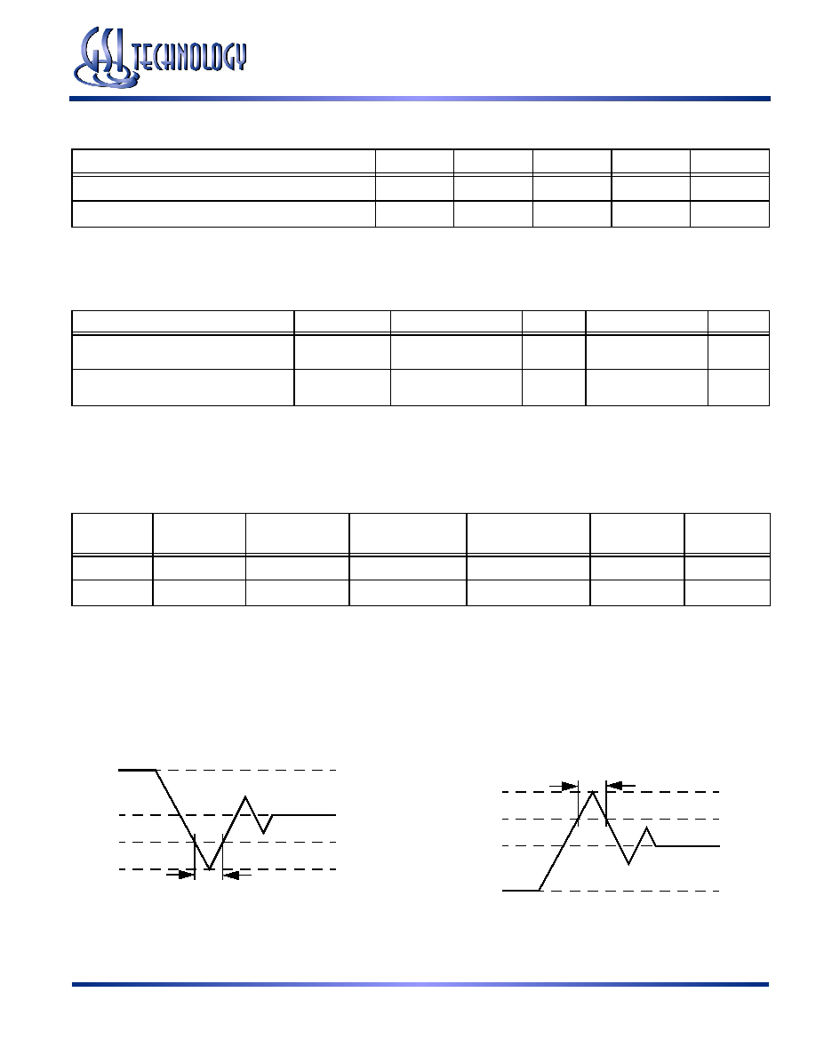
20% tKC
VSS – 2.0 V
50%
VSS
VIH
Undershoot Measurement and Timing
Overshoot Measurement and Timing
20% tKC
VDD + 2.0 V
50%
VDD
VIL
Note:
Input Under/overshoot voltage must be –2 V > Vi < VDDn+2 V not to exceed 4.6 V maximum, with a pulse width not to exceed 20% tKC.
相關PDF資料 |
PDF描述 |
|---|---|
| GS832472GC-150I | 512K X 72 CACHE SRAM, 10 ns, PBGA209 |
| GS832472GC-250T | 512K X 72 CACHE SRAM, 6 ns, PBGA209 |
| GS8342D08E-333T | 4M X 8 STANDARD SRAM, 0.45 ns, PBGA165 |
| GS8342Q08AE-278 | 4M X 8 DDR SRAM, 0.45 ns, PBGA165 |
| GS84018AB-190 | 256K X 18 CACHE SRAM, 7.5 ns, PBGA119 |
相關代理商/技術參數(shù) |
參數(shù)描述 |
|---|---|
| GS832236AB-333 | 制造商:GSI Technology 功能描述:119 BGA - Bulk |
| GS832236AB-333I | 制造商:GSI Technology 功能描述:119 BGA - Bulk |
| GS832236AB-375 | 制造商:GSI Technology 功能描述:119 BGA - Bulk |
| GS832236AB-375I | 制造商:GSI Technology 功能描述:119 BGA - Bulk |
| GS832236AB-375M | 制造商:GSI Technology 功能描述:119 BGA - Bulk |
發(fā)布緊急采購,3分鐘左右您將得到回復。