- 您現(xiàn)在的位置:買賣IC網(wǎng) > PDF目錄384353 > GS841Z18AT-150I (GSI TECHNOLOGY) 4Mb Pipelined and Flow Through Synchronous NBT SRAMs PDF資料下載
參數(shù)資料
| 型號: | GS841Z18AT-150I |
| 廠商: | GSI TECHNOLOGY |
| 元件分類: | DRAM |
| 英文描述: | 4Mb Pipelined and Flow Through Synchronous NBT SRAMs |
| 中文描述: | 256K X 18 ZBT SRAM, 10 ns, PQFP100 |
| 封裝: | TQFP-100 |
| 文件頁數(shù): | 11/30頁 |
| 文件大小: | 495K |
| 代理商: | GS841Z18AT-150I |
第1頁第2頁第3頁第4頁第5頁第6頁第7頁第8頁第9頁第10頁當前第11頁第12頁第13頁第14頁第15頁第16頁第17頁第18頁第19頁第20頁第21頁第22頁第23頁第24頁第25頁第26頁第27頁第28頁第29頁第30頁
GS841Z18/36AT-180/166/150/100
Specifications cited are subject to change without notice. For latest documentation see http://www.gsitechnology.com.
Rev: 1.02 11/2004
11/30
2001, GSI Technology
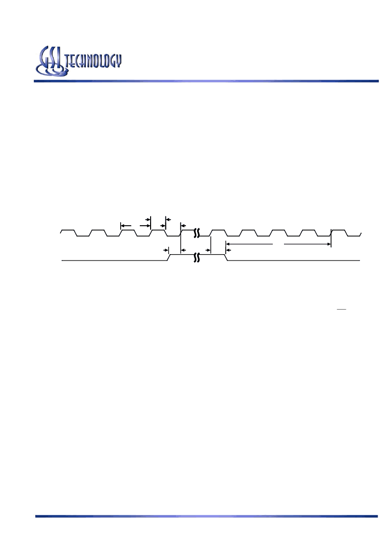
Sleep Mode
During normal operation, ZZ must be pulled low, either by the user or by its internal pull down resistor. When ZZ is pulled high,
the SRAM will enter a Power Sleep mode after 2 cycles. At this time, internal state of the SRAM is preserved. When ZZ returns to
low, the SRAM operates normally after 2 cycles of wake up time.
Sleep mode is a low current, power-down mode in which the device is deselected and current is reduced to I
SB
2. The duration of
Sleep mode is dictated by the length of time the ZZ is in a High state. After entering Sleep mode, all inputs except ZZ become
disabled and all outputs go to High-Z The ZZ pin is an asynchronous, active high input that causes the device to enter Sleep mode.
When the ZZ pin is driven high, I
SB
2 is guaranteed after the time tZZI is met. Because ZZ is an asynchronous input, pending
operations or operations in progress may not be properly completed if ZZ is asserted. Therefore, Sleep mode must not be initiated
until valid pending operations are completed. Similarly, when exiting Sleep mode during tZZR, only a Deselect or Read commands
may be applied while the SRAM is recovering from Sleep mode.
Sleep Mode Timing Diagram
Designing for Compatibility
The GSI NBT SRAMs offer users a configurable selection between Flow Through mode and Pipeline mode via the FT signal
found on Pin 14. Not all vendors offer this option, however most mark Pin 14 as V
DD
or V
DDQ
on pipelined parts and V
SS
on flow
through parts. GSI NBT SRAMs are fully compatible with these sockets.
Pin 66, a No Connect (NC) on GSI’s GS840Z18/36 NBT SRAM, the Parity Error open drain output on GSI’s GS841Z18/36 NBT
SRAM, is often marked as a power pin on other vendor’s NBT-compatible SRAMs. Specifically, it is marked V
DD
or V
DDQ
on
pipelined parts and V
SS
on flow through parts. Users of GSI NBT devices who are not actually using the ByteSafe parity feature
may want to design the board site for the RAM with Pin 66 tied high through a 1k ohm resistor in Pipeline mode applications or
tied low in Flow Through mode applications in order to keep the option to use non-configurable devices open. By using the pull-up
resistor, rather than tying the pin to one of the power rails, users interested in upgrading to GSI’s ByteSafe NBT SRAMs
(GS841Z18/36), featuring Parity Error detection and JTAG Boundary Scan, will be ready for connection to the active low, open
drain Parity Error output driver at Pin 66 on GSI’s TQFP ByteSafe RAMs.
tZZR
tZZH
tZZS
tKL
tKH
tKC
CK
ZZ
相關(guān)PDF資料 |
PDF描述 |
|---|---|
| GS841Z18AT-166 | 4Mb Pipelined and Flow Through Synchronous NBT SRAMs |
| GS841Z18AT-166I | 4Mb Pipelined and Flow Through Synchronous NBT SRAMs |
| GS841Z18AT-180 | 4Mb Pipelined and Flow Through Synchronous NBT SRAMs |
| GS841Z18AT-180I | 4Mb Pipelined and Flow Through Synchronous NBT SRAMs |
| GS841Z36AGT-100 | 4Mb Pipelined and Flow Through Synchronous NBT SRAMs |
相關(guān)代理商/技術(shù)參數(shù) |
參數(shù)描述 |
|---|---|
| GS841Z18AT-166 | 制造商:GSI 制造商全稱:GSI Technology 功能描述:4Mb Pipelined and Flow Through Synchronous NBT SRAMs |
| GS841Z18AT-166I | 制造商:GSI 制造商全稱:GSI Technology 功能描述:4Mb Pipelined and Flow Through Synchronous NBT SRAMs |
| GS841Z18AT-180 | 制造商:GSI 制造商全稱:GSI Technology 功能描述:4Mb Pipelined and Flow Through Synchronous NBT SRAMs |
| GS841Z18AT-180I | 制造商:GSI 制造商全稱:GSI Technology 功能描述:4Mb Pipelined and Flow Through Synchronous NBT SRAMs |
| GS841Z18CGT-150 | 制造商:GSI Technology 功能描述:2.5 OR 3.3V - Trays |
發(fā)布緊急采購,3分鐘左右您將得到回復(fù)。