- 您現(xiàn)在的位置:買賣IC網(wǎng) > PDF目錄223866 > GS8662QT10BD-200I (GSI TECHNOLOGY) 8M X 9 QDR SRAM, 0.45 ns, PBGA165 PDF資料下載
參數(shù)資料
| 型號: | GS8662QT10BD-200I |
| 廠商: | GSI TECHNOLOGY |
| 元件分類: | SRAM |
| 英文描述: | 8M X 9 QDR SRAM, 0.45 ns, PBGA165 |
| 封裝: | 13 X 15 MM, 1 MM PITCH, FPBGA-165 |
| 文件頁數(shù): | 1/29頁 |
| 文件大小: | 303K |
| 代理商: | GS8662QT10BD-200I |
當前第1頁第2頁第3頁第4頁第5頁第6頁第7頁第8頁第9頁第10頁第11頁第12頁第13頁第14頁第15頁第16頁第17頁第18頁第19頁第20頁第21頁第22頁第23頁第24頁第25頁第26頁第27頁第28頁第29頁
GS8662QT07/10/19/37BD-357/333/300/250/200
72Mb SigmaQuad-II+TM
Burst of 2 SRAM
357 MHz–200 MHz
1.8 V VDD
1.8 V and 1.5 V I/O
165-Bump BGA
Commercial Temp
Industrial Temp
Rev: 1.00 5/2011
1/29
2011, GSI Technology
Specifications cited are subject to change without notice. For latest documentation see http://www.gsitechnology.com.
Features
2.0 Clock Latency
Simultaneous Read and Write SigmaQuad Interface
JEDEC-standard pinout and package
Dual Double Data Rate interface
Byte Write controls sampled at data-in time
Dual-Range On-Die Termination (ODT) on Data (D), Byte
Write (BW), and Clock (K, K) inputs
Burst of 2 Read and Write
1.8 V +100/–100 mV core power supply
1.5 V or 1.8 V HSTL Interface
Pipelined read operation
Fully coherent read and write pipelines
ZQ pin for programmable output drive strength
Data Valid Pin (QVLD) Support
IEEE 1149.1 JTAG-compliant Boundary Scan
165-bump, 13 mm x 15 mm, 1 mm bump pitch BGA package
RoHS-compliant 165-bump BGA package available
SigmaQuad Family Overview
The GS8662QT07/10/19/37BD are built in compliance with
the SigmaQuad-II+ SRAM pinout standard for Separate I/O
synchronous SRAMs. They are 75,497,472-bit (72Mb)
SRAMs. The GS8662QT07/10/19/37BD SigmaQuad SRAMs
are just one element in a family of low power, low voltage
HSTL I/O SRAMs designed to operate at the speeds needed to
implement economical high performance networking systems.
Clocking and Addressing Schemes
The GS8662QT07/10/19/37BD SigmaQuad-II+ SRAMs are
synchronous devices. They employ two input register clock
inputs, K and K. K and K are independent single-ended clock
inputs, not differential inputs to a single differential clock input
buffer.
Because Separate I/O SigmaQuad-II+ B2
RAMs always
transfer data in two packets, A0 is internally set to 0 for the
first read or write transfer, and automatically incremented by 1
for the next transfer. Because the LSB is tied off internally, the
address field of a SigmaQuad-II+ B2
RAM is always one
address pin less than the advertised index depth (e.g., the 4M x
18 has a 2M addressable index).
Parameter Synopsis
-357
-333
-300
-250
-200
tKHKH
2.8 ns
3.0 ns
3.3 ns
4.0 ns
5.0 ns
tKHQV
0.45 ns
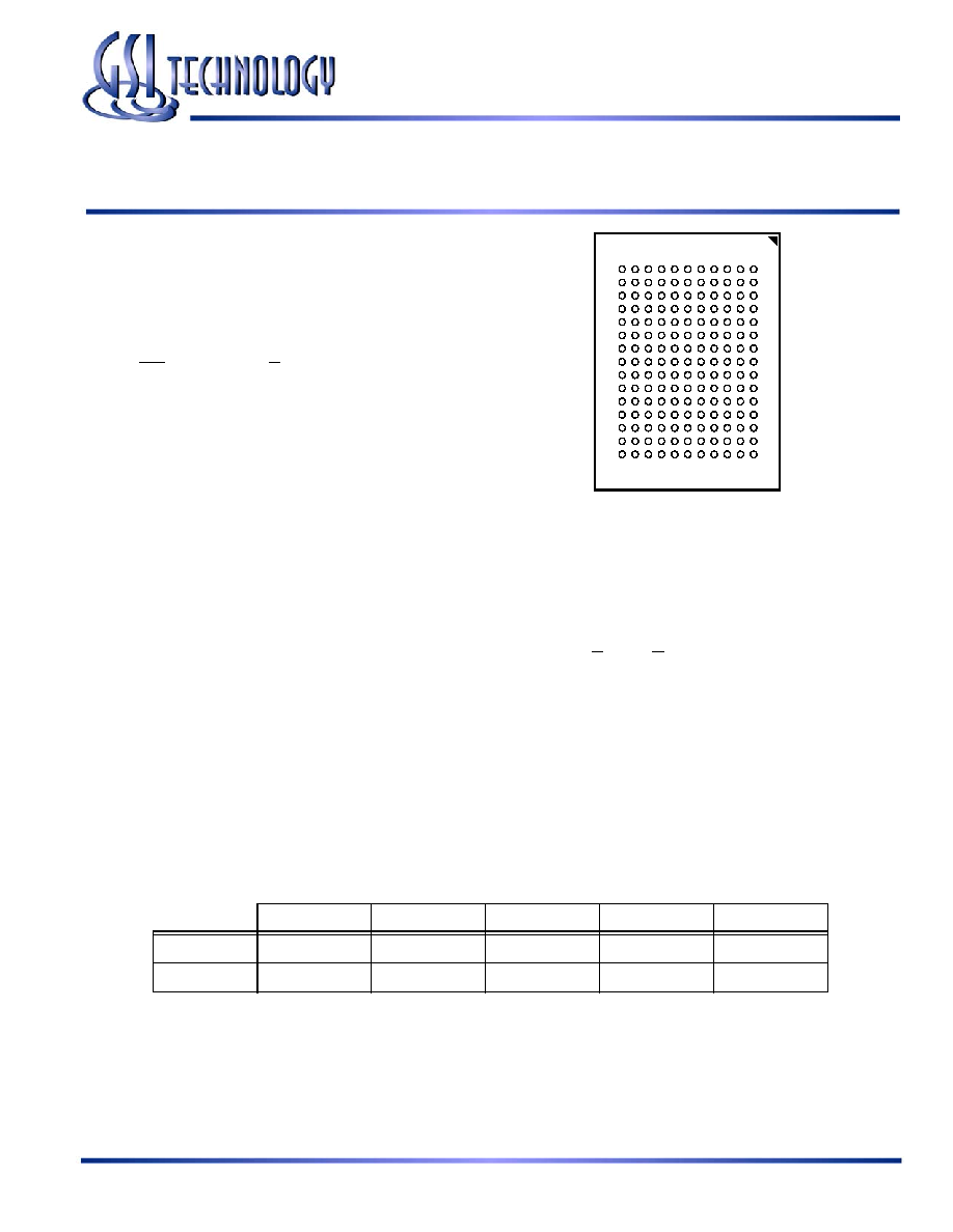
165-Bump, 13 mm x 15 mm BGA
1 mm Bump Pitch, 11 x 15 Bump Array
Bottom View
相關(guān)PDF資料 |
PDF描述 |
|---|---|
| GS8662QT10BGD-250T | 8M X 9 QDR SRAM, 0.45 ns, PBGA165 |
| GS8662T06BD-350I | 8M X 8 DDR SRAM, 0.45 ns, PBGA165 |
| GS8662T06BD-350T | 8M X 8 DDR SRAM, 0.45 ns, PBGA165 |
| GS8672Q38BE-500I | 2M X 36 QDR SRAM, 0.45 ns, PBGA165 |
| GS880F32AGT-5.5IT | 256K X 32 CACHE SRAM, 5.5 ns, PQFP100 |
相關(guān)代理商/技術(shù)參數(shù) |
參數(shù)描述 |
|---|---|
| GS8662R08BD-167 | 制造商:GSI Technology 功能描述:GS8662R08BD-167 - Trays |
| GS8662R08BD-200 | 制造商:GSI Technology 功能描述:GS8662R08BD-200 - Trays |
| GS8662R08BD-200I | 制造商:GSI Technology 功能描述:GS8662R08BD-200I - Trays |
| GS8662R08E | 制造商:GSI 制造商全稱:GSI Technology 功能描述:72Mb SigmaCIO DDR-II Burst of 4 SRAM |
| GS8662R08E-167 | 制造商:GSI 制造商全稱:GSI Technology 功能描述:72Mb SigmaCIO DDR-II Burst of 4 SRAM |
發(fā)布緊急采購,3分鐘左右您將得到回復(fù)。