- 您現(xiàn)在的位置:買賣IC網(wǎng) > PDF目錄383055 > GS9010ACTC (Electronic Theatre Controls, Inc.) Serial Digital Automatic Tuning Subsystem PDF資料下載
參數(shù)資料
| 型號: | GS9010ACTC |
| 廠商: | Electronic Theatre Controls, Inc. |
| 英文描述: | Serial Digital Automatic Tuning Subsystem |
| 中文描述: | 串行數(shù)字自動調(diào)諧子系統(tǒng) |
| 文件頁數(shù): | 6/6頁 |
| 文件大小: | 169K |
| 代理商: | GS9010ACTC |
6
521 - 01 - 05
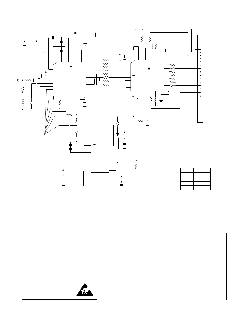
STANDARD TRUTH TABLE
/2 P/N STANDARD
0 0 4:2:2 - 270
0 1 4:2:2 - 360
1 0 4sc - NTSC
1 1 4sc - PAL
P/N
OUT
IN-
COMP
LF
/2
VCC
SWF
1
2
3
4
5
6
7
8
16
15
14
13
12
11
10
9
PARALLEL DATA BIT 9
PARALLEL DATA BIT 8
PARALLEL DATA BIT 7
PARALLEL DATA BIT 6
PARALLEL DATA BIT 5
PARALLEL DATA BIT 4
PARALLEL DATA BIT 3
PARALLEL DATA BIT 2
PARALLEL DATA BIT 1
PARALLEL DATA BIT 0
PARALLEL CLOCK OUT
SYNC CORRECTION ENABLE
HSYNC OUTPUT
SYNC WARNING FLAG
INPUT SELECTION
STDT
VCC
CD
HSYNC
GND
OSC
DLY
FVCAP
10
μ
+
10
μ
10
μ
+
+
V
CC
+5V
+5V
V
CC
V
CC
V
CC
0.1
μ
100
100
100
100
390
390
390
390
0.1
μ
0.1
μ
0.1
μ
25
24
23
22
21
20
19
5
6
7
8
9
10
11
4 3 2 1 28 27 26
V
12 13 14 15 16 17 18
910
(1)
(2)
(2)
(2)
(3)
75
113
75
47p
0.1
μ
0.1
μ
3.3n
82n
180n
0.68
μ
0.1
μ
DGND
DGND
DGND
DGND
0.1
μ
DGND
GND
1.2k
100
120
50k
0.1
μ
0.1
μ
F
100k
DD
I
DD
I
VCC2
SD
I
SD
I
/2
VEE3
SDO
SDO
SCO
SCO
SS1
SS0
CD
V
A
A
S
I
V
V
L
R
R
R
E
R
V
25
24
23
22
21
20
19
5
6
7
8
9
10
11
4 3 2 1 28 27 26
S
0.1
μ
DGND
DGND
SSI
100
100
100
100
3.3k
100
100
100
100
GS9000B
or GS9000S
SD
I
SD
I
SC
I
SC
I
SS1
SS0
SST
PD7
PD6
PD5
PD4
PD3
PD2
PD1
V
V
V
H
P
P
V
V
V
S
S
P
P
STAR
ROUTED
12 13 14 15 16 17
V
CC
V
CC
V
CC
V
CC
6.8
μ
6.8
μ
+
+
GS9005A
V
CC
V
CC
DV
CC
DV
CC
DV
CC
V
CC
DV
CC
V
CC
(4)
SWF
SWF
Gennum Corporation assumes no responsibility for the use of any circuits described herein and makes no representations that they are free from patent infringement.
Copyright January 1994 Gennum Corporation. All rights reserved. Printed in Canada.
REVISION NOTES
Figures 1 and 3 updated
(1) Typical value for input return loss matching
(2) To reduce board space, the two anti-series 6.8
μ
F capacitors (connected across pins 2 and 3 of the GS9010A)
may be replaced with a 1.0
μ
F non-polarized capacitor provided that:
(a) the 0.68
μ
F capacitor connected to the OSC pin (11) of the GS9010A is replaced with a 0.33
μ
F capacitor and
(b) the GS9005A /15A Loop Filter Capacitor is 10 nF.
(3) Remove this potentiometer if P/N function is not required, and ground pin 16 of the GS9010A.
(4) The GS9000B will operate to a maximum frequency of 370 Mbps.
The GS9000S will operate to a maximum frequency of 300 Mbps.
All resistors in ohms, all capacitors in microfarads, all inductors in henries unless otherwise stated.
Fig. 3 Typical Application Circuit
DOCUMENT
IDENTIFICATION
PRODUCT PROPOSAL
This data has been compiled for market investigation purposes
only, and does not constitute an offer for sale.
ADVANCE INFORMATION NOTE
This product is in development phase and specifications are
subject to change without notice. Gennum reserves the right to
remove the product at any time. Listing the product does not
constitute an offer for sale.
PRELIMINARY
The product is in a preproduction phase and specifications are
subject to change without notice.
DATA SHEET
The product is in production. Gennum reserves the right to
make changes at any time to improve reliability, function or
design, in order to provide the best product possible.
CAUTION
ELECTROSTATIC
SENSITIVE DEVICES
DO NOT OPEN PACKAGES OR HANDLE
EXCEPT AT A STATIC-FREE WORKSTATION
相關(guān)PDF資料 |
PDF描述 |
|---|---|
| GS9015A | Serial Digital Reclocker |
| GS9015ACPJ | Serial Digital Reclocker |
| GS9015ACTJ | Serial Digital Reclocker |
| GS9025A | Serial Digital Receiver |
| GS9025ACQM | Serial Digital Receiver |
相關(guān)代理商/技術(shù)參數(shù) |
參數(shù)描述 |
|---|---|
| GS9010CKC | 制造商:未知廠家 制造商全稱:未知廠家 功能描述:Analog IC |
| GS9010CTC | 制造商:GENNUM 功能描述:* |
| GS9012 | 制造商:未知廠家 制造商全稱:未知廠家 功能描述:TRANSISTOR | BJT | PNP | 20V V(BR)CEO | 500MA I(C) | TO-226AA |
| GS9012/E6 | 制造商:未知廠家 制造商全稱:未知廠家 功能描述:BJT |
| GS9012/E7 | 制造商:未知廠家 制造商全稱:未知廠家 功能描述:BJT |
發(fā)布緊急采購,3分鐘左右您將得到回復(fù)。